

4-BIT MAGNITUDE COMPARATOR
.EXPANSION TO 8, 12, 16 ... 4 N BITSBY CAS-
CADING UNITS
.MEDIUM-SPEED OPERATION : COMPARES
TWO 4-BIT WORDS IN 180ns (typ.) AT 10V
.STANDARDIZED SYMMETRICAL OUTPUT
CHARACTERISTICS
.5V, 10V, AND 15VPARAMETRIC RATINGS
.INPUT CURRENTOF100nA AT18VAND25°C
FOR HCC DEVICE
.100% TESTEDFOR QUIESCENTCURRENT
.MEETSALLREQUIREMENTSOFJEDECTEN-
TATIVESTANDARDN°13A,”STANDARD SPECIFICATIONS FOR DESCRIPTION OF ”B”
SERIESCMOS DEVICES”
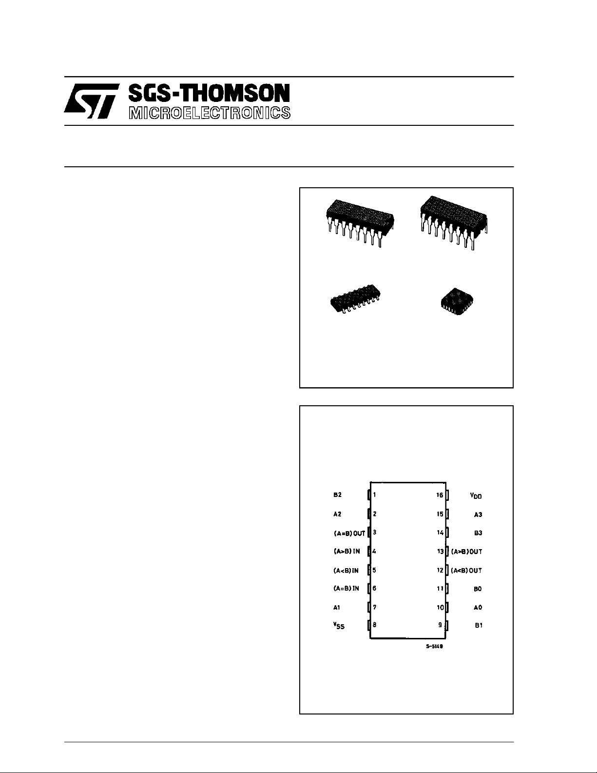
HCC/HCF4585B
EY
(Plastic Package)F(Ceramic FritSealPackage)
M1
(MicroPackage)
ORDER CODES :
HCC4585BF HCF4585BM1
HCF4585BEY HCF4585BC1
(PlasticChip Carrier)
C1
DESCRIPTI ON
TheHCC4585B (extended temperature range) and
HCF4585B (intermediate temperature range) are
monolithic integrated circuits, available in 16-lead
dual in-line plastic or ceramic package, and plastic
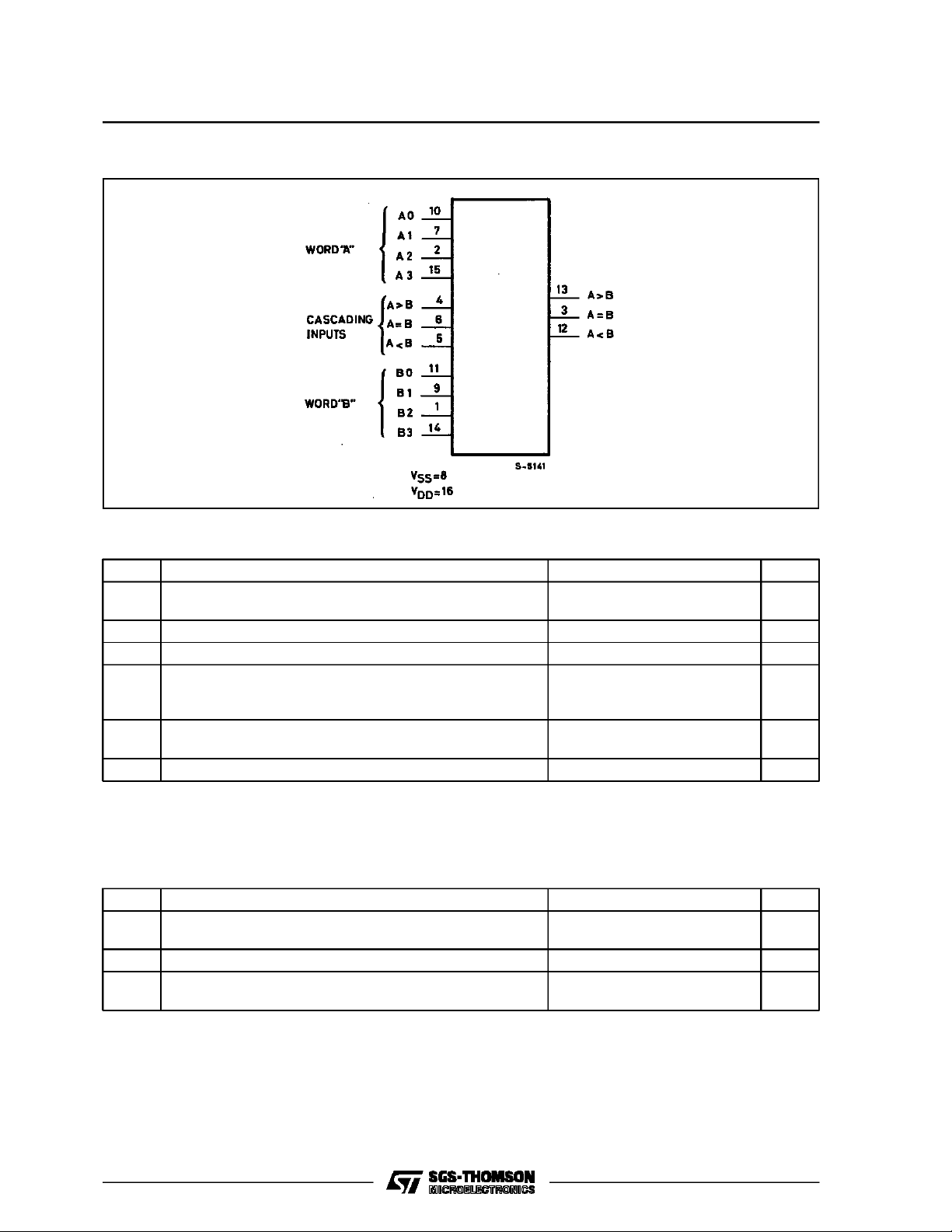
micropackage.TheHCC/HCF4585B isa4-bitmag-
nitudecomparator designed foruseincomputer and
logicapplications that require thecomparison of two
4-bit words. This logic circuit determines whether
one 4-bit word(BinaryorBCD)is”less than”, ”equal
to”, or ”greater than” a second 4-bit word. The
HCC/HCF4585B has eight comparing inputs (A3,
B3,throughA0, B0),threeoutputs(A<B, A= B, A>
B) and three cascadinginputs (A < B, A = B, A > B)
that permit systems designers to expand the comparator function to 8, 12, 16 ... 4 N bits. When a
single HCC/HCF4585B is used, the cascading inputs are connected as follows : (A < B) = low,
(A =B) =high, (A> B)= high.Cascadingthese units
for comparison of more than 4 bits is accomplished
as shownin typicalapplication.
PIN CONNECTIONS
June1989
1/12
HCC/HCF4585B
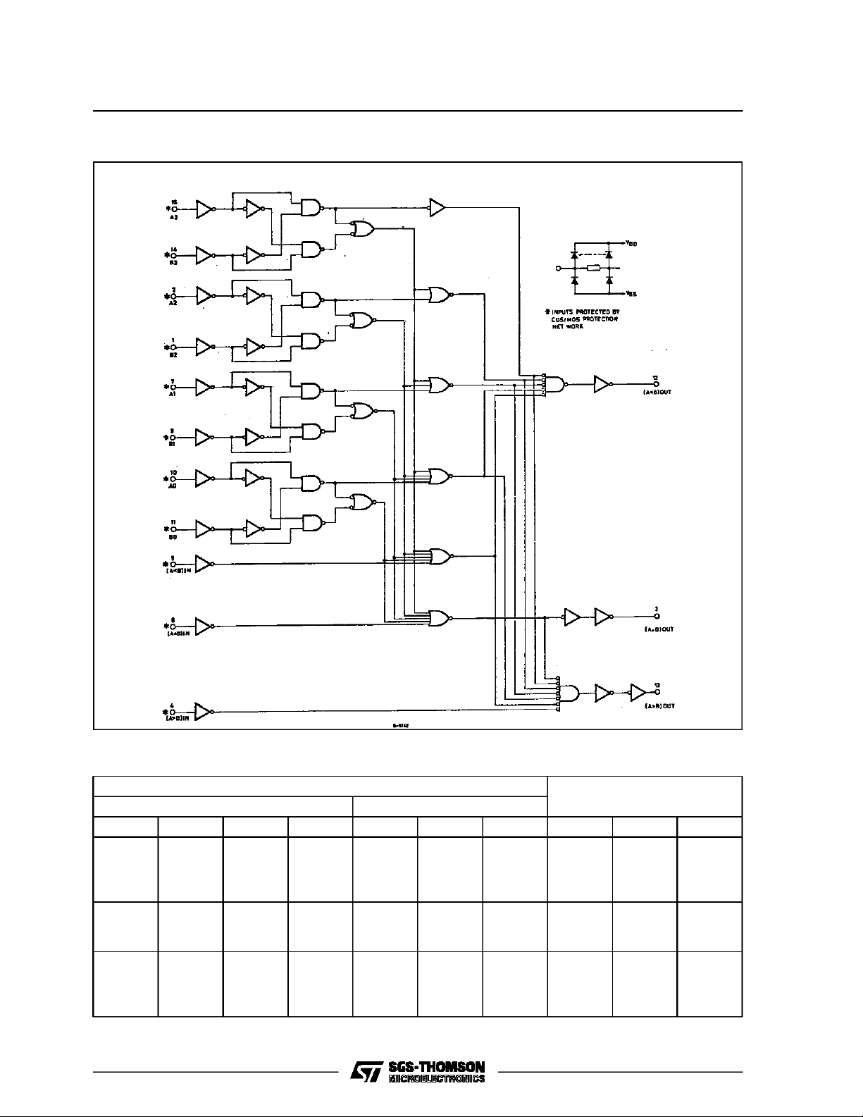
FUN CTIONAL DIAG R A M
ABSOLUTE MAXIMUM RATIN G S
Symbol Parameter Value Unit
V
* Supply Voltage :HC C Types
DD
HCF Types
V
Input Voltage – 0.5 to VDD+ 0.5 V
i
I
DC Input Current (any one input) ± 10 mA
I
P
Total Power Dissipation (per package)
tot
– 0.5 to + 20
– 0.5 to + 18
200
V
V
mW
Dissipation per Output Transistor
for T
T
T
Stresses above those listed under ”Absolute Maximum Ratings” may cause permanent damage to the device. This is a stress
rating only and functional operation of the device at these or any other conditions above those indicated in the operational sections
of this specification is not implied. Exposure to absolute maximum rating conditions for external periods may affect device reliability.
* All voltages are with respect to VSS(GND).
Operating Temperature : HCC Types
op
Storage Temperature – 65 to + 150 °C
stg
= Full Package-temperature Range
op
HCF Types
100
– 55 to + 125
–40to+85
mW
°C
°C
RECOMMENDED OPERATING C ONDITIONS
Symbol Parameter Value Unit
V
T
Supply Voltage : HCC Types
DD
HCF Types
V
Input Voltage 0 to V
I
Operating Temperature : HCC Types
op
HCF Types
3to18
3to15
DD
– 55 to + 125
–40to+85
V
V
V
°C
°C
2/12
LOGI C DI AGRAM
HCC/HCF4585B
TRUTH TABLE
Inputs
Comparing Cascadi ng
A3, B3 A2, B2 A1, B1 A0, B0 A < B A = B A > B A < B A = B A > B
A3 > B3
A3 = B3
A3 = B3
A3 = B3
A3 = B3
A3 = B3
A3 = B3
A3 = B3
A3 = B3
A3 = B3
A3 < B3
X = Don’t C ar e Logic 1 = Hi gh Level
X
A2 > B2
A2 = B2
A2 = B2
A2 = B2
A2 = B2
A2 = B2
A2 = B2
A2 = B2
A2 < B2
X
X
X
A1 > B1
A1 = B1
A1 = B1
A1 = B1
A1 = B1
A1 = B1
A1 < B1
X
X
X
X
X
A0 > B0
A0 = B0
A0 = B0
A0 = B0
A0 < B0
X
X
X
X
X
X
X
0
0
1
X
X
X
X
X
X
X
X
0
1
0
X
X
X
X
1
1
1
1
1
X
X
X
X
X
X
0
0
0
0
0
0
1
1
1
1
1
Outputs
0
0
0
0
0
1
0
0
0
0
0
1
1
1
1
1
0
0
0
0
0
0
3/12
HCC/HCF4585B
STATIC ELECTRICAL CHARACTERISTICS (over recommended operatingconditions)
Test Conditions Valu e
Symbol Parameter
I
Quiescent
L
Current
HCC
Types
HCF
Types
V
OH
Output High
Voltage
V
OL
Output Low
Voltage
V
IH
Input High
Voltage
IL
Input Low
V
Voltage
I
OH
Output
Drive
Current
HCC
Types
HCF
Types
I
OL
Output
Sink
Current
HCC
Types
HCF
Types
I
IH,IIL
Input
Leakage
Current
HCC
Types
HCF
Types
C
Input Capacitance Any Input 5 7.5 pF
I
*T
=–55°CforHCC device : – 40°CforHCF device.
Low
*T
= + 125°CforHCC device : + 85°CforHCF device.
High
The Noise Margin for both ”1” and ”0” level is : 1V min. with VDD= 5V, 2V min. with VDD= 10V, 2.5V min. with VDD= 15V.
V
V
O
|IO|V
I
(V) (V) (µA) (V)
T
DD
* 25°CT
Low
Min. Max. Min. Ty p. Max. Min. Max .
High
*
0/ 5 5 5 0.04 5 150
0/10 10 10 0.04 10 300
0/15 15 20 0.04 20 600
0/20 20 100 0.08 100 3000
0/ 5 5 20 0.04 20 150
0/10 10 40 0.04 40 300
0/15 15 80 0.04 80 600
0/ 5 < 1 5 4.95 4.95 4.95
0/10 < 1 10 9.95 9.95 9.95
0/15 < 1 15 14.95 14.95 14.95
5/0 < 1 5 0.05 0.05 0.05
10/0 < 1 10 0.05 0.05 0.05
15/0 < 1 15 0.05 0.05 0.05
0.5/4.5 < 1 5 3.5 3.5 3.5
1/9 < 1 10 7 7 7
1.5/13.5 < 1 15 11 11 11
4.5/0.5 < 1 5 1.5 1.5 1.5
9/1 < 1 10 3 3 3
13.5/1.5 < 1 15 4 4 4
0/ 5 2.5 5 – 2 – 1.6 – 3.2 – 1.15
0/ 5 4.6 5 – 0.64 – 0.51 – 1 – 0.36
0/10 9.5 10 – 1.6 – 1.3 – 2.6 – 0.9
0/15 13.5 15 – 4.2 – 3.4 – 6.8 – 2.4
0/ 5 2.5 5 – 1.53 – 1.36 – 3.2 – 1.1
0/ 5 4.6 5 – 0.52 – 0.44 – 1 – 0.36
0/10 9.5 10 – 1.3 – 1.1 – 2.6 – 0.9
0/15 13.5 15 – 3.6 – 3.0 – 6.8 – 2.4
0/ 5 0.4 5 0.64 0.51 1 0.36
0/10 0.5 10 1.6 1.3 2.6 0.9
0/15 1.5 15 4.2 3.4 6.8 2.4
0/ 5 0.4 5 0.52 0.44 1 0.36
0/10 0.5 10 1.3 1.1 2.6 0.9
0/15 1.5 15 3.6 3.0 6.8 2.4
0/18
18
± 0.1 ±10
–5
± 0.1 ± 1
Any Input
0/15
15 ± 0.3 ±10
–5
± 0.3 ± 1
Unit
µA
V
V
V
V
mA
mA
µA
4/12

HCC/HCF4585B
DYNAMIC ELECTRICAL CHARACTERISTICS (T
=25°C, CL= 50pF, RL= 200kΩ,
amb
typical temperature coefficient for all VDDvalues is 0.3%/°C, all input rise and fall time = 20ns)
Symbol Parameter
t
,
PHL
t
PLH
Propagation Delay Time
Comparing Inputs to Outputs
Cascading Input to Outputs 5 200 400
t
,
THL
t
TLH
Transition Time 5 100 200
Test Conditions Value
(V) Min. Typ. Max.
V
DD
5300600
10 125 250
15 80 160
10 80 160
15 60 120
10 50 100
15 40 80
OutputLow (sink) Current Characteristics. OutputHigh (source) Current Characteristics.
Unit
ns
ns
ns
TypicalTransitionTime vs. Load Capacitance. Typical Propagation Delay Time (comparing in-
puts to outputs)vs. Load Capacitance.
5/12

HCC/HCF4585B
TypicalDynamicPower Dissipation vs. Clock
Input Frequency.
TYPICAL APPLICA TION
TYPICALSPEED CHARACTERISTICS OF A 12-BITCOMPARATOR
6/12

TEST CIRCUITS
QuiescentDevice Current. Input Voltage.
Input Leakage Current. DynamicPower Dissipation.
HCC/HCF4585B
7/12
HCC/HCF4585B
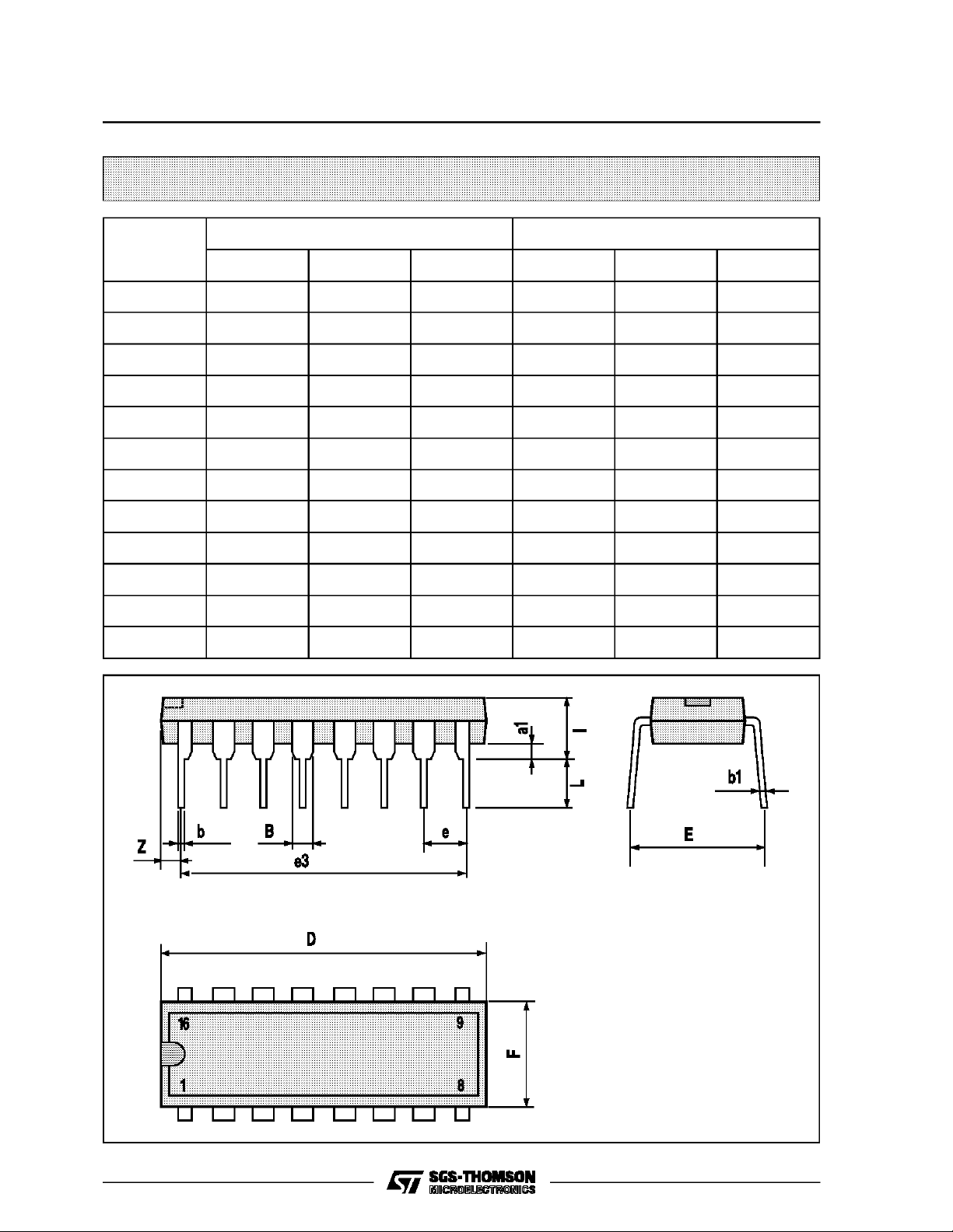
Plastic DIP16 (0.25) MECHANICAL DATA
DIM.
MIN. TYP. MAX. MIN. TYP. MAX.
a1 0.51 0.020
B 0.77 1.65 0.030 0.065
b 0.5 0.020
b1 0.25 0.010
D 20 0.787
E 8.5 0.335
e 2.54 0.100
e3 17.78 0.700
F 7.1 0.280
I 5.1 0.201
L 3.3 0.130
Z 1.27 0.050
mm inch
8/12
P001C

Ceramic DIP16/1 MECHANICAL DATA
HCC/HCF4585B
DIM.
MIN. TYP. MAX. MIN. TYP. MAX.
A 20 0.787
B 7 0.276
D 3.3 0.130
E 0.38 0.015
e3 17.78 0.700
F 2.29 2.79 0.090 0.110
G 0.4 0.55 0.016 0.022
H 1.17 1.52 0.046 0.060
L 0.22 0.31 0.009 0.012
M 0.51 1.27 0.020 0.050
N 10.3 0.406
P 7.8 8.05 0.307 0.317
Q 5.08 0.200
mm inch
P053D
9/12

HCC/HCF4585B
SO16 (Narrow) MECHANICAL DATA
DIM.
MIN. TYP. MAX. MIN. TYP. MAX.
A 1.75 0.068
a1 0.1 0.2 0.004 0.007
a2 1.65 0.064
b 0.35 0.46 0.013 0.018
b1 0.19 0.25 0.007 0.010
C 0.5 0.019
c1 45° (typ.)
D 9.8 10 0.385 0.393
E 5.8 6.2 0.228 0.244
e 1.27 0.050
e3 8.89 0.350
F 3.8 4.0 0.149 0.157
G 4.6 5.3 0.181 0.208
L 0.5 1.27 0.019 0.050
M 0.62 0.024
S8°(max.)
mm inch
10/12
P013H

PLCC20 MECHANICAL DATA
HCC/HCF4585B
DIM.
MIN. TYP. MAX. MIN. TYP. MAX.
A 9.78 10.03 0.385 0.395
B 8.89 9.04 0.350 0.356
D 4.2 4.57 0.165 0.180
d1 2.54 0.100
d2 0.56 0.022
E 7.37 8.38 0.290 0.330
e 1.27 0.050
e3 5.08 0.200
F 0.38 0.015
G 0.101 0.004
M 1.27 0.050
M1 1.14 0.045
mm inch
P027A
11/12

HCC/HCF4585B
Information furnished is believed to be accurate and reliable.However, SGS-THOMSON Microelectronics assumes no responsability for the
consequences of use of such information nor for any infringement of patents or other rights of third parties which may results from its use. No
license is granted by implication or otherwise underany patent or patent rights of SGS-THOMSON Microelectronics. Specificationsmentioned
in this publicationare subject to changewithout notice.This publication supersedes and replaces all information previously supplied.
SGS-THOMSON Microelectronicsproductsare notauthorized for use ascritical componentsin life supportdevices or systems without express
written approval of SGS-THOMSON Microelectonics.
1994SGS-THOMSON Microelectronics- All Rights Reserved
Australia - Brazil - France - Germany - HongKong - Italy - Japan - Korea - Malaysia - Malta - Morocco - The Netherlands -
Singapore - Spain - Sweden - Switzerland -Taiwan - Thailand - UnitedKingdom - U.S.A
SGS-THOMSON Microelectronics GROUP OF COMPANIES
12/12
 Loading...