

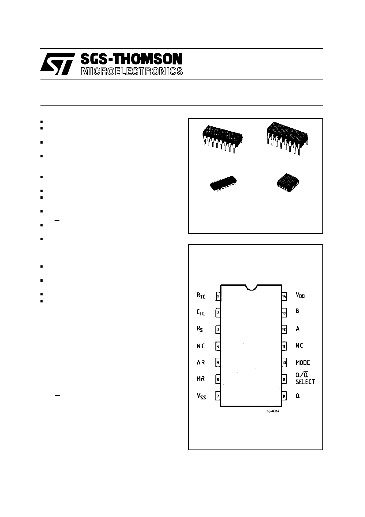
16 STAGEBINARI COUNTER
LOWSYMMETRICALOUTPUT RESISTANCE,
TYPICALLY 100 OHM ATVDD=15V
OSCILLATOR FREQUENCY RANGE : DC TO
100kHz
AUTOOR MASTER RESET DISABLES OSCILLATORDURINGRESET TOREDUCE POWER
DISSIPATION
OPERATESWITH VERY SLOW CLOCK RISE
AND FALL TIMES
BUILT-INLOW-POWER RC OSCILLATOR
EXTERNAL CLOCK (applied to pin 3) CAN BE
USEDINSTEAD OF OSCILLATOR
OPERATESAS 2NFREQUENCY DIVIDER OR
AS A SINGLE-TRANSITION TIMER
Q/Q SELECT PROVIDES OUTPUT LOGIC
LEVELFLEXIBILITY
CAPABLEOF DRIVINGSIXLOW POWERTTL
LOADS, THREE LOW-POWER SCHOTTKY
LOADS, PR SIX HTL LOADS OVER THE
RATEDTEMPERATURE RANGE
SYMMETRICAL OUTPUT CHARACTERISTICS
100% TESTED FOR QUIESCENT CURRENT
AT 20V
5-10-15VPARAMETRICRATINGS
MEETSALLREQUIREMENTSOFJEDECTENTATIVESTANDARD N13A, ”STANDARDSPECIFICATIONS FOR DESCRIPTION OF ’ B ’
SERIESCMOS DEVICES”
HCC4 54 1B
HCF4541B
PROGRAMMABLE TIMER
EY
(Plastic Package)
M1
(Micro Package)
ORDER CODE S :
HCC 4541 BF HCF4541 BM 1
HCF4541 BE Y HCF4541 BC1
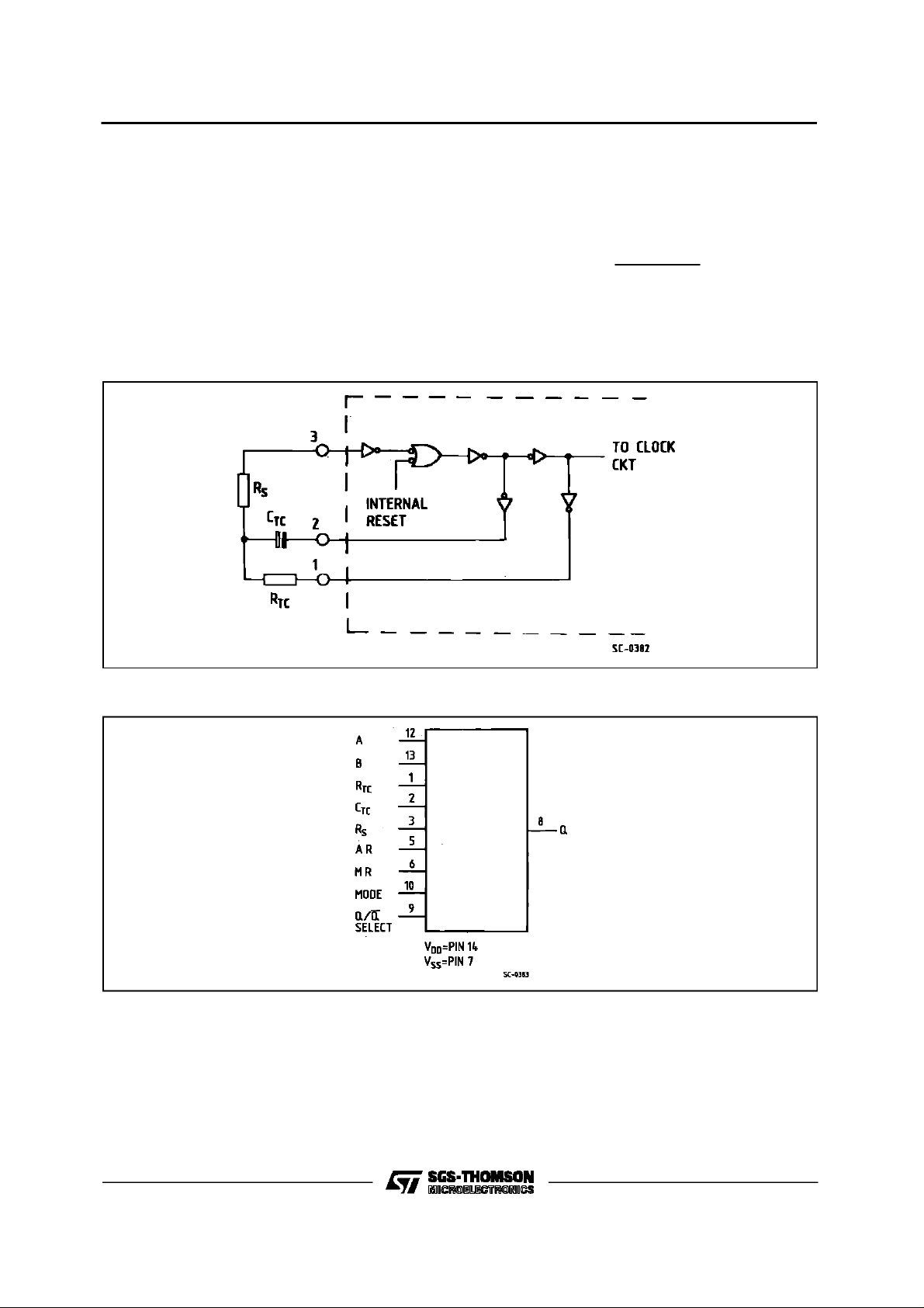
PIN CO NNECTION (top vie w)
(Ceramic Frit Seal Package)
(Plastic Chip Carrier)
F
C1
DESCRI PTION
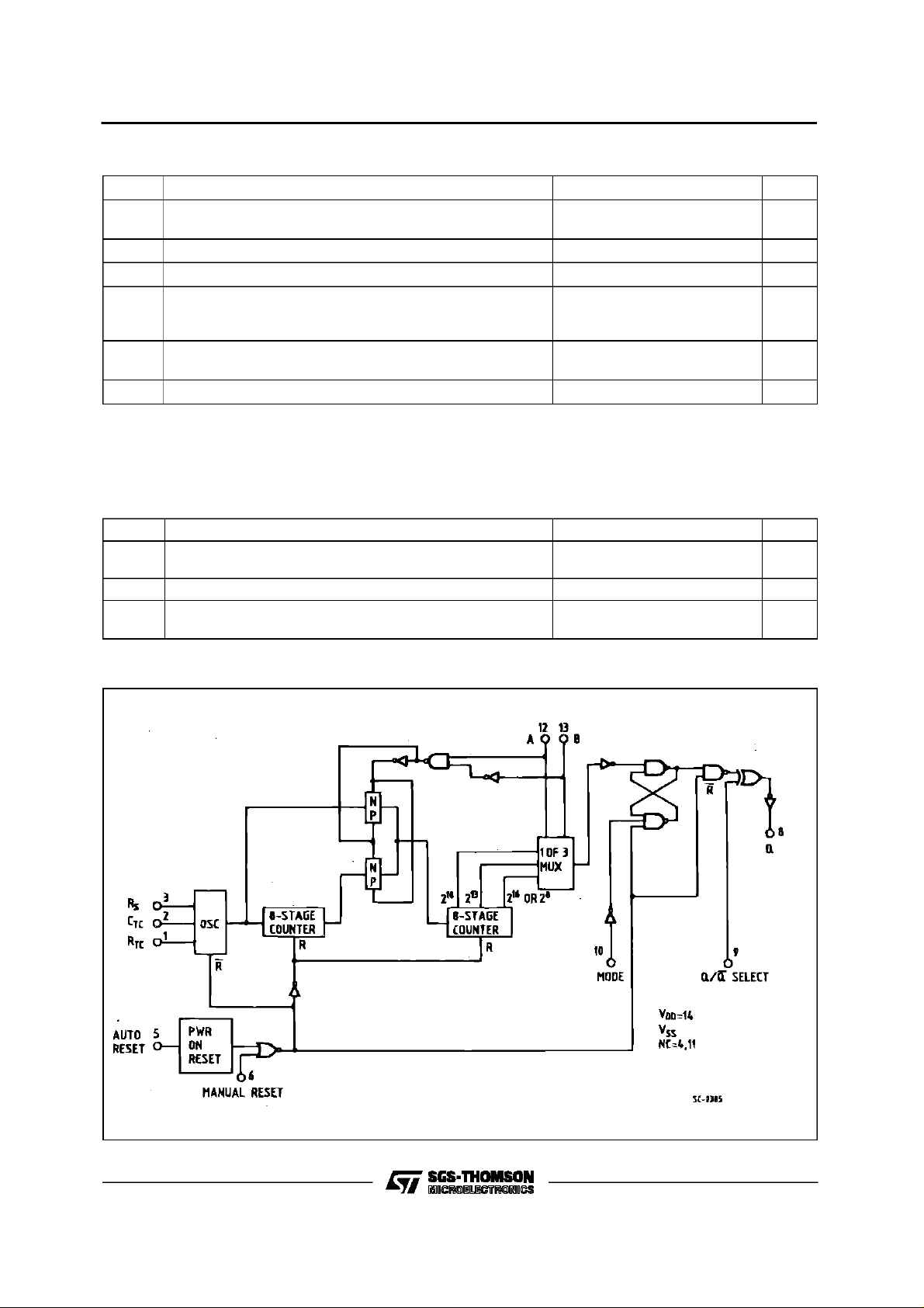
TheHCC/HCF4541B Programmable Timeriscomposed of a 16-stage binary counter, an oscillator
controlled by2 externalresistorsand a capacitor,an
output control logic and an automatic power-on
reset circuit. The counter varies on positive-edge
clocktransation and it can be cleared by the MASTER RESETinput.The outputfrom thistimer is the
Q or Q output from the 8th, 13th, or 16th counter
stage.Thechoice ofthestagedepends on thetimeselectinputsA or B (seefrequency selection table).
The output isavailable inone ofthe two modes that
can be selected via the MODE input, pin 10 (see
truth table). The output turns out as a continuous
squarewave,with afrequencyequaltotheoscillator
frequency divided by 2N. When this MODE input is
November1996
1/11
HCC/HCF4541B
a logic” 1 ”, whenit is a logic ” 0 ” andafter a MASTER RESET is started, and Q output has been selected, the output goes up to a high stateafter 2
N-1
counts.It remainsin thatstate till anotherMASTER
RESETpulse is apply or the mode inputis a logic ”
1 ”. Theprocess starts bysettingtheAUTO RESET
input(pin 5) to logic ” 0 ” and switching poweron. If
pin 5 is setto logic ”1 ”, the AUTORESETcircuitis
not enabled and counting cannot start till a positive
MASTERRESETpulse isapplied, returningtoalow
level. The AUTO RESET consumes a remarkable
RC OscillatorCircuit.
amount of power and should not be used if lowpoweroperation is wanted.
The frequency of the oscillator depends on the RC
network. Itcanbe calculated usingthefollowing formula:
f =
1
2.3 RTCC
TC
wheref is between 1 kHz and 100 kHz
and RS ≥ 10 kΩ and ≈ 2R
TC
FUNCTIONAL DIAGRAM
2/11
HCC/HCF4541B
ABSOLU TE M AXIMU M R AT INGS
Symbol Parameter Value Unit
* Supply Voltage: HCC Types
V
DD
HCF Types
Input Voltage – 0.5to VDD+ 0.5 V
V
I
I
DC Input Current (anyone input) ± 10 mA
I
Total Power Dissipation (perpackage)
P
tot
Dissipation per Output Transistor
for T
= FullPackage-temperature range
op
T
Operating Temperature : HCC Types
op
HCF Types
T
Storage Temperature – 65to + 150 °C
stg
Stresses above those listed under ” Absolute Maximum Ratings ” may cause permanent damage to the device. This is a stress
rating only and functional operation of the device at these or any other conditions above those indicated in the operational sections of this specification is not implied. Exposure to absolute maximum rating conditions for extended periods may affect device
reliability.
* All voltages are with respect to VSS(GND).
RECO MM ENDED OPERAT IN G CO NDITI ONS
Symbol Paramet er Value Unit
Supply Voltage : HCC Types
V
DD
InputVoltage 0 to V
V
I
Operating Temperature : HCC Types
T
op
HCF Types
HCF Types
– 0.5to + 20
– 0.5to + 18
200
100
– 55to + 125
–40to+85
3to 18
3to 15
DD
– 55to 125
–40to85
V
V
mW
mW
°C
°C
V
V
V
°C
°C
LOGI C DI AGRAM
3/11
HCC/HCF4541B
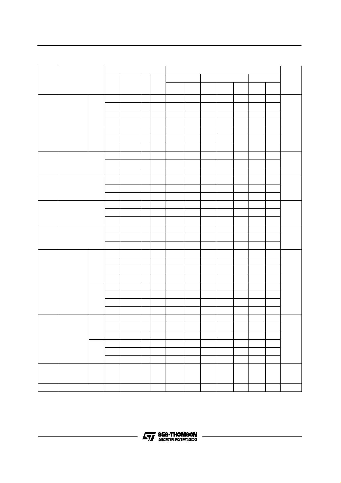
STATIC ELECTRICAL
Test Conditions Value
I
Symbol Parameter
Quiescent
I
L
Current
HCC
Types
V
(V)
V
I
(V)
0/5 5 5 0.04 5 150
0/10 10 10 0.04 10 300
0/15 15 20 0.04 20 600
O
(uA
)
V
(V)
DD
O
0/20 20 100 0.08 100 3000
0/5 5 5 0.04 5 150
HCF
Types
0/10 10 10 0.04 10 300
0/15 15 20 0.04 20 600
V
OH
OutputHigh
Voltage
0/5 < 1 5 4.95 4.95 4.95
0/10 < 1 10 9.95 9.95 9.95
0/15 < 1 15 14.95 14.95 14.95
V
OL
OutputLow
Voltage
5/0 < 1 5 0.05 0.05 0.05
10/0 < 1 10 0.05 0.05 0.05
15/0 < 1 15 0.05 0.05 0.05
V
IH
InputHigh
Voltage
0.5/4.5 < 1 5 3.5 3.5 3.5
1/9 < 1 10 7 7 7
1.5/13.5 < 1 15 11 11 11
V
IL
InputLow
Voltage
4.5/0.5 < 1 5 1.5 1.5 1.5
9/1 < 1 10 3 3 3
13.5/1.5 < 1 15 4 4 4
Output
I
OH
Drive
Current
HCC
Types
0/5 4.6 5 – 1.9 – 1.55 – 3.1 – 1.08
0/5 2.5 5 – 6.2 – 5 – 10 – 3
0/10 9.5 10 – 5.0 – 4 – 8 – 2.8
0/15 13.5 15 – 12.6 – 10 – 20 – 7.2
0/5 4.6 5 – 1.85 – 1.55 – 3.1 – 1.26
0/5 2.5 5 – 6.0 – 5 – 10 – 4.1
HCF
Types
0/10 9.5 10 – 4.8 – 4 – 8 – 3.3
0/15 13.5 15 – 12 – 10 – 20 – 8.4
Output
I
OL
Sink
Current
HCC
Types
0/5 0.4 5 1.9 1.55 3.1 1.08
0/10 0.5 10 5.0 4 8 2.8
0/15 1.5 15 12.6 10 20 7.2
0/5 0.4 5 1.85 1.55 3.1 1.26
HCF
Types
0/10 0.5 10 4.8 4 8 3.3
0/15 1.5 15 12 10 20 8.4
Input
I
IH,IIL
Leakage
0/18 Any Input 18 ± 0.1
Current
InputCapacitance Any Input 5 7.5 pF
C
I
*T
= - 55C for HCC device : - 40C for HCF device.
Low
*T
= + 125C for HCC device : + 85C for HCF device.
High
The Noise Margin for both ” 1 ” and ” 0 ” level is : 1V min. with VDD= 5V 2V min. with VDD= 10V 2.5V min. with VDD=15V
T
Low
25°CT
High
Min. Max. Min. Typ. Max. Min. Max.
–
± 0.1
± 0.1 ± 1 µA
5
Unit
µA
V
V
V
V
mA
mA
4/11

HCC/HCF4541B
DYNAMICELECTRICAL CHARACTERISTICS (T
=25°C, CL= 50pF, RL=200kΩ,
amb
typicaltemperature coefficient for allVDDvalues is 0.3%/°C, all input riseand fall time = 20ns)
Symbol Parameter
8
(2
)
Propagation Delay Time
t
Clock toQ
PHL
t
PLH
16
)
(2
t
PHL
t
PLH
Transition Time 5 100 200
t
THL
t
TLH
Master Reset,Clock Pulse Width 5 900 300
f
Maximum Clock Pulse Input Frequency 5 1.5
CL
tr,tf Maximum Clock Pulse InputRise or FallTime 5
VDD
(V)
5 3.5 10.5
10 1.25 3.8
15 0.9 2.9
5618
10 3.5 10
15 2.5 7.5
10 50 100
15 40 80
5 180 360
10 90 180
15 65 130
10 300 100
15 225 85
10 4
15 6
10
15
Values
Min. Typ. Max.
Unlimited µs
Unit
µs
µs
ns
ns
MHz
5/11

HCC/HCF4541B
DIGITAL TIMER A PPLICATION
A positive MASTER RESET pulse clears the
counters andlatch.The outputgoeshighand keeps
up tillthenumber ofpulses,selected byAandB, are
counted.Thiscircuitis retriggerable andisas accurate as theinputfrequency. If amoreaccuratecircuit
is desired, an external clock can be used on pin 3.
A set-uptime equal tothe width oftheone shot output is required immediately following initial power
up, during which time theoutput will be high.
FREQUENC Y S ELECT ION TA BL E TRUTH TABLE
AB
0 0 13 8192
0 1 10 1024
1 0 18 256
1 1 16 65536
N°of Stages
N
Count
N
2
Pin
5 Auto Reset On AutoReset Disable
6 MasterReset Off Master Reset On
9
Low After Reset (Q)
10 SingleTransition Mode Recycle Mode
01
OutputInitially
State
OutputInitially
HighAfter Reset (Q)
6/11

Plastic DIP14 MECHANICAL DATA
HCC/HCF4541B
DIM.
MIN. TYP. MAX. MIN. TYP. MAX.
a1 0.51 0.020
B 1.39 1.65 0.055 0.065
b 0.5 0.020
b1 0.25 0.010
D 20 0.787
E 8.5 0.335
e 2.54 0.100
e3 15.24 0.600
F 7.1 0.280
I 5.1 0.201
L 3.3 0.130
Z 1.27 2.54 0.050 0.100
mm inch
P001A
7/11

HCC/HCF4541B
Ceramic DIP14/1 MECHANICAL DATA
DIM.
MIN. TYP. MAX. MIN. TYP. MAX.
A 20 0.787
B 7.0 0.276
D 3.3 0.130
E 0.38 0.015
e3 15.24 0.600
F 2.29 2.79 0.090 0.110
G 0.4 0.55 0.016 0.022
H 1.17 1.52 0.046 0.060
L 0.22 0.31 0.009 0.012
M 1.52 2.54 0.060 0.100
N 10.3 0.406
P 7.8 8.05 0.307 0.317
Q 5.08 0.200
mm inch
8/11
P053C

SO14 MECHANICAL DATA
HCC/HCF4541B
DIM.
MIN. TYP. MAX. MIN. TYP. MAX.
A 1.75 0.068
a1 0.1 0.2 0.003 0.007
a2 1.65 0.064
b 0.35 0.46 0.013 0.018
b1 0.19 0.25 0.007 0.010
C 0.5 0.019
c1 45° (typ.)
D 8.55 8.75 0.336 0.344
E 5.8 6.2 0.228 0.244
e 1.27 0.050
e3 7.62 0.300
F 3.8 4.0 0.149 0.157
G 4.6 5.3 0.181 0.208
L 0.5 1.27 0.019 0.050
M 0.68 0.026
S8°(max.)
mm inch
P013G
9/11

HCC/HCF4541B
PLCC20 MECHANICAL DATA
DIM.
MIN. TYP. MAX. MIN. TYP. MAX.
A 9.78 10.03 0.385 0.395
B 8.89 9.04 0.350 0.356
D 4.2 4.57 0.165 0.180
d1 2.54 0.100
d2 0.56 0.022
E 7.37 8.38 0.290 0.330
e 1.27 0.050
e3 5.08 0.200
F 0.38 0.015
G 0.101 0.004
M 1.27 0.050
M1 1.14 0.045
mm inch
10/11
P027A

HCC/HCF4541B
Information furnished is believed to be accurate and reliable. However, SGS-THOMSON Microelectronics assumes no responsability for the
consequences of use of such informationnor for any infringement of patents or other rights of third parties which may results from its use. No
licenseis grantedby implication or otherwise under any patentor patent rights of SGS-THOMSONMicroelectronics. Specifications mentioned
in this publication aresubject to changewithout notice. Thispublication supersedes and replacesall informationpreviouslysupplied.
SGS-THOMSONMicroelectronics products are not authorized for use ascriticalcomponents in lifesupport devices or systemswithout express
writtenapproval ofSGS-THOMSON Microelectonics.
1996 SGS-THOMSON Microelectronics - Printedin Italy- AllRights Reserved
Australia- Brazil - Canada - China - France- Germany - HongKong- Italy - Japan- Korea-Malaysia - Malta - Morocco - The Netherlands -
Singapore - Spain - Sweden - Switzerland- Taiwan - Thailand- UnitedKingdom - U.S.A
SGS-THOMSONMicroelectronics GROUPOF COMPANIES
.
11/11
 Loading...