

DUAL MONOSTABLE MULTIVIBRATOR
.RETRIGGERABLE/RESETTABLE
CAPABILITY
.TRIGGER AND RESET PROPAGATION DE-
LAYS INDEPENDENT OF RX,C
X
.TRIGGERING FROM LEADING OR TRAILING
EDGE
.Q AND Q BUFFERED OUTPUTSAVAILABLE
.SEPARATE RESETS
.WIDE RANGEOF OUTPUT-PULSE WIDTHS
.QUIESCENT CURRENT SPECIFIED TO 20V
FOR HCC DEVICE
.5V, 10V,AND 15V PARAMETRIC RATINGS
.SCHMITT TRIGGER INPUT ALLOWS UN-
LIMITERRISEANDFALL TIMES ON+ TRAND
– TR INPUTS
.INPUT CURRENTOF 100nA AT 18VAND 25°C
FOR HCC DEVICE
.100% TESTEDFOR QUIESCENTCURRENT
.MEETSALLREQUIREMENTSOFJEDECTEN-
TATIVESTANDARDN°13A,”STANDARDSPECIFICATIONS FOR DESCRIPTION OF ”B”
SERIESCMOS DEVICES”
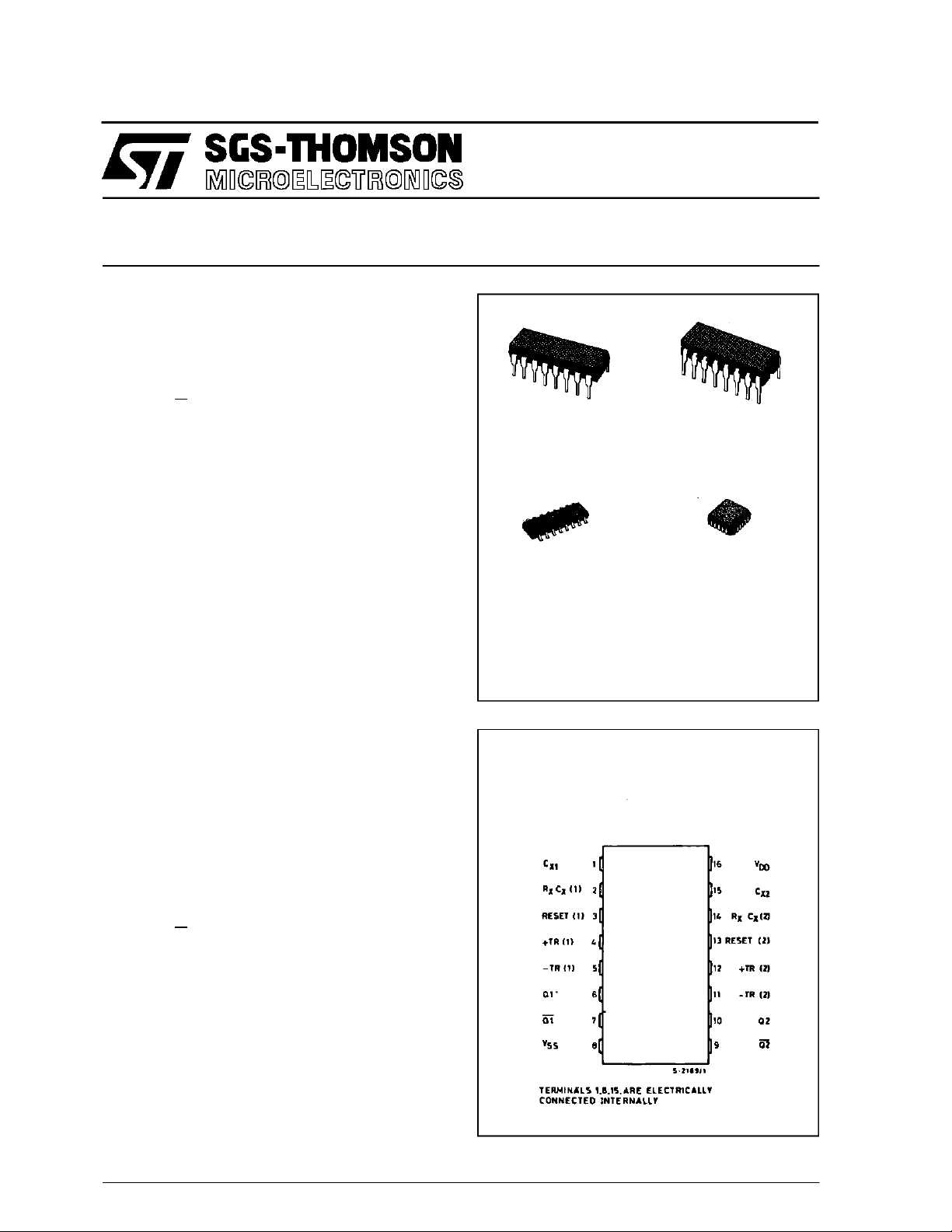
HCC4538B
HCF4538B
EY
(PlasticPackage)
M1
(MicroPackage)
ORDER CODES :
HCC4 538BF HCF4538BM1
HCF4538BEY HCF4538BC1
(CeramicPackage)
(Chip Carrier)
F
C1
DESCRIPTION
TheHCC4538B (extended temperature range) and
HCF4538B (intermediate temperature range) are
monolithic integrated circuit, available in 16-lead
dual in-line plastic or-ceramic package and plastic
micropackage.TheHCC/HCF4538Bdualprecision
monostable multivibrator provides stable retriggerable/resettable one-shot operation for any fixedvoltage timing application. An external resistor (RX)
andanexternalcapacitor(CX) controlthetimingand
accuracy for the circuit. Adjustment of RXand C
provides a wide range of output pulse widths from
the Q and Q terminals. The timedelay from trigger
inputtooutput transition (trigger propagation delay)
and the time delayfrom reset input to output transition(resetpropagation delay)are independent ofR
and CX. Precision control of output pulse widths is
achieved through linear CMOS techniques. Leading-edge-triggering (+TR)and trailing-edge-triggering (– TR) inputs are provided for triggering from
eitheredge of aninput pulse. Anunused+TR input
shouldbe tiedto VSS. An unused– TRinput should
be tied to VDD. A RESET (on low level) is provided
for immediate termination of the output pulse or to
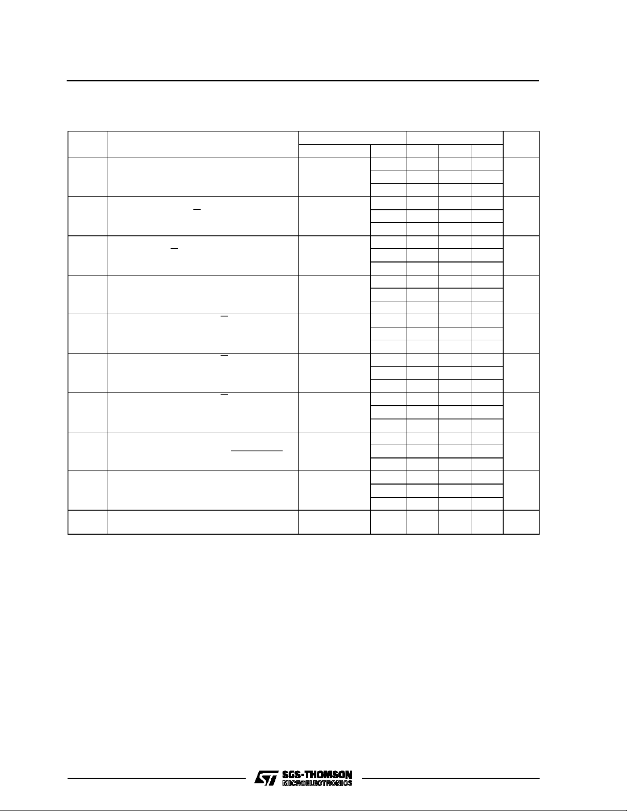
PIN CONNECTIONS
X
X
September 1988
1/14

HCC/HCF4538B
prevent output pulses when power is turnedon. An
unused RESET input should be tied to VDD. However, if an entire section of the HCC/HCF4538B is
not used,itsinputsmustbe tiedto eitherVDDor V
SS
(see table1).In normal operationthe circuittriggers
(extends the output pulse one period) on the applicationofeachnewtriggerpulse. Foroperation inthe
non-retriggerable mode, Q is connected to – TR
FUN CTIONAL DIAG R A M
whenleading-edge triggering (+TR) is used or Q is
connected to + TR when trailingedge triggering (–
TR)isused.Thetimeperiod(T) forthismultivibrator
can be calculated by : T = RXCX. The min. value of
externalresistance,RX,is4KΩ. The max. and min.
values of external capacitance, CX, are100µF and
5nF,respectively.
ABSOLU TE MAXIMU M RAT ING
Symbol Parameter Value Unit
* Supply Voltage: HCC Types
V
DD
HCF Types
V
P
Input Voltage -0.5 to VDD+ 0.5 V
i
I
DC Input Current (any one input) ± 10 mA
I
Total Power Dissipation (per package)
tot
-0.5 to +20
-0.5 to +18
200
V
V
mW
Dissipation per Output Transistor
for Top = Full Package Temperature Range
T
Operating Temperature: HCC Types
op
HCF Types
T
Stressesabove those listedunder”AbsoluteMaximum Ratings”maycausepermanent damagetothedevice.Thisisastressratingonlyand functional
operation of the device at these or any otherconditions above thoseindicated in theoperational sections of thisspecificationisnotimplied.Exposure
to absolute maximum ratingconditionsforexternal periods mayaffect device reliability.
* All voltagevalues are referred to VSSpinvoltage.
Storage Temperature -65 to +150
stg
100
-55 to +125
-40 to +85
mW
o
C
o
C
o
C
RECO MM ENDED OPERATIN G C O NDITIONS
Symbol Parameter Value Unit
V
Supply Voltage: HCC Types
DD
HCF Types
V
T
Input Voltage 0 to V
I
Operating Temperature: HCC Types
op
HCF Types
3to18
3to15
DD
-55 to +125
-40 to +85
V
V
V
o
C
o
C
2/14

LOGI C DIAGRAM (1/2 of device s hown)
HCC/HCF4538B
TABLE 1: F uncti onal Terminal C onnections
to Term. NO VSSto Term. NO
V
DD
Function
Mono
(1)
Leading-Edge
Trigger/Retriggerable
Leading-Edge
Trigger/Non-retriggerable
Trailing-Edge
Trigger/Retriggerable
Trailing-Edge
Trigger/Non-retriggerable
Notes : 1. A Retriggerable one-shot multivibrator has an outputpulsewidth which is extended onfulltime period(T)afterapplication of the last
triggerpulse.
2. A Non-retriggerable one-shot multivibratorhasa time period (T) referenced fromthe application of the first trigger pulse.
3, 5 11, 13 4 12
3 13 4 12 5, 7 11, 9
313412511
3 13 5 11 4, 6 12, 10
Mono
(2)
Mono
(1)
Mono
(2)
Input Pulse to
Term. No
Mono
(1)
Mono
(2)
Other
Connections
Mono
(1)
Mono
(2)
Pulse Width
3/14

HCC/HCF4538B
STATI C ELECT RIC AL CHAR ACTER I STI CS (ov er recomm end ed op er a ting conditi ons)
Test Conditios Value
Symbol Parameter
Quiescent
I
L
Current
HCC
Types
V
(V)
V
I
(V)
|IO|
(µA)
V
(V)
O
T
DD
*25
LOW
Min. Max. Min. Typ. Max. Min. Max.
0/5 5 5 0.04 5 150
0/10 10 10 0.04 10 300
0/15 15 20 0.04 20 600
o
CT
0/20 20 100 0.08 100 3000
HCF
Types
0/5 5 5 0.04 5 150
0/10 10 10 0.04 10 300
0/15 15 20 0.04 20 600
OH
Output High
V
Voltage
0/5 < 1 5 4.95 4.95 5 4.95
0/10 < 1 10 9.95 9.95 10 9.95
0/15 < 1 15 14.95 14.95 15 14.95
OL
Output Low
V
Voltage
5/0 < 1 5 0.05 0.05 0.05
10/0 < 1 10 0.05 0.05 0.05
15/0 < 1 15 0.05 0.05 0.05
IH
Input High
V
Voltage
0.5/4.5 < 1 5 3.5 3.5 3.5
1/9 < 1 10 7 7 7
1.5/13.5 < 1 15 11 11 11
IL
Input Low
V
Voltage
4.5/0.5 < 1 5 1.5 1.5 1.5
9/1 < 1 10 3 3 3
13.5/1.5 < 1 15 4 4 4
OH
Output
Drive
Current
HCC
Types
I
0/5 2.5 5 -2 -1.6 -3.2 -1.15
0/5 4.6 5 -0.64 -0.51 -1 -0.36
0/10 9.5 10 -1.6 -1.3 -2.6 -0.9
0/15 13.5 15 -4.2 -3.4 -6.8 -2.4
0/5 2.5 5 -1.8 -1.6 -3.2 -1.3
HCF
Types
0/5 4.6 5 -0.61 -0.51 -1 -0.42
0/10 9.5 10 -1.5 -1.3 -2.6 -1.1
0/15 13.5 15 -4 -3.4 -6.8 -2.8
I
OL
Output
Sink
Current
HCC
Types
HCF
Types
0/5 0.4 5 0.64 0.51 1 0.36
0/10 0.5 10 1.6 1.3 2.6 0.9
0/15 1.5 15 4.2 3.4 6.8 2.4
0/5 0.4 5 0.61 0.51 1 0.42
0/10 0.5 10 1.5 1.3 2.6 1.1
0/15 1.5 15 3.6 3.4 6.8 2.8
I
IH,IIL
C
*T
LOW
*T
HIGH
TheNoiseMargin for both ”1” and ”0” level is: 1V min. withVDD=5V,2 V min.withVDD=10V,2.5 V min. withVDD=15V
Input Leakage
Current
Input Capacitance Any Input 5 7.5 pF
I
=-55oCforHCC device: -40oC for HCF device.
=+125oCfor HCCdevice:+85oC for HCF device.
0/18 Any Input 18 ±0.1 ±10
-5
±0.1 ±1 µA
HIGH
Unit
*
µA
V
V
V
V
mA
mA
4/14
HCC/HCF4538B
DYNAMIC ELECTRICAL CHARACTERISTICS (T
=25oC, CL=50pF,RL= 200 KΩ,
amb
typic al tem perat ur e coefficent for all VDDvalues is 03 %/oC, all input rise and fall t im es = 20 ns)
Symbol Parameter
t
t
t
t
t
t
t
t
t
t
TLH
THL
PLH
PHL
PLH
PHL
WH
Transition Time 5 100 200
Propagation Delay Time
+TR or -TR to Q or Q
Propagation Delay Time
Reset to Q or Q
Minimum Input Pulse Width
+TR, -TR or Reset
WL
Output Pulse Width - Q or Q
WT
(C
= 0.005 µF, RX=10KΩ*)
X
Output Pulse Width - Q or Q
WT
(CX= 0.1 µF, RX= 100 KΩ)
t
Output Pulse Width - Q or Q
WT
(CX=10µF, RX= 100 KΩ)
t
Pulse Width Match Between
W
Circuits in Same Package:
100 (
(CX= 0.1 µF, RX= 100 KΩ)
t
Minimum Retrigger Time 5 0
rr
C
* MinimumRXvalue=4 KΩ,minimum CXvalue= 500 pF
Input Capacitance Any
IN
T
−
T
)
1
2
T
1
Test Conditions Value
(V) Min. Typ. Max.
V
DD
10 50 100
15 40 80
5 300 600
10 150 300
15 100 220
RL=1KΩ 5 250 500
10 125 250
15 95 190
RL=1KΩ 5 80 140
10 40 80
15 30 60
5 57 60.6 64.5
10 55 58.9 63.0
15 55 59.1 63.5
5 9.4 9.97 10.5
10 9.4 9.95 10.6
15 9.5 10.00 10.6
5 0.95 1.00 1.06
10 0.95 1.00 1.06
15 0.96 1.00 1.07
5 ±1
10 ±1
15 ±1
10 0
15 0
5 7.5 pF
Input
Unit
ns
ns
ns
ns
µs
ms
s
%
ns
5/14

HCC/HCF4538B
Typical Output Low (sink) Current Characteristics
Typical Output High (source) Current Characteristics
Minimum Output Low (sink) Current Characteristics
Minimum Output High (source) Current Characteristics
Typical Propagation Delay Time as a Function of
Load Capacitance (+TR or -TR to Q or Q)
6/14
Typical Propagation Delay TIme as a Function of
Load Capacitance (RESET to Q or Q)

HCC/HCF4538B
Typical Transition Time as a Function of Load
Capacitance
Typical Pulse Width Variation as a Function of
Temperature
Typical Pulse Width Variation as a Function of
Supply Voltage
Typical Pulse Width Variation as a Function of
Temeprature
Typical Total Supply Current as a Function of
Output Duty Cycle
7/14

HCC/HCF4538B
Power Down Mode
During a rapid power-down conditiona, as would
occur with a power supply short circuit or with a
poorlyfilteredpower supply, theenergy storedinC
coulddischarge intoPin 2 or 14. To Avoid possible
devicedamage inthismode,whenCXis≤0.5microfarad,a aprotectiondiode witha 1Ampereorhigher
An alternate protection method is shown in Fig. 2,
where a 51 Ω current limit resistor is inserted in
series with CX. Note that a small pulse width de-
X
creasewilloccour however, and RXmust be appropriately increased to obtain the originally desired
pulsewidth.
rating (1N5395 or equivalent) and a separate
groundreturn for CXshould be provided as shown
in Fig. 1
Figure 1: rapid Power Down Protection Circuit Figure 2: Alternate rapid Power Down Protection
Circuit
8/14

TEST CIRCUITS
QuiescentDevice Current. Noise Immunity.
Input Leakage Current.
HCC/HCF4538B
9/14

HCC/HCF4538B
Plastic DIP16 (0.25) MECHANICAL DATA
DIM.
MIN. TYP. MAX. MIN. TYP. MAX.
a1 0.51 0.020
B 0.77 1.65 0.030 0.065
b 0.5 0.020
b1 0.25 0.010
D 20 0.787
E 8.5 0.335
e 2.54 0.100
e3 17.78 0.700
F 7.1 0.280
I 5.1 0.201
L 3.3 0.130
Z 1.27 0.050
mm inch
10/14
P001C

Ceramic DIP16/1 MECHANICAL DATA
HCC/HCF4538B
DIM.
MIN. TYP. MAX. MIN. TYP. MAX.
A 20 0.787
B 7 0.276
D 3.3 0.130
E 0.38 0.015
e3 17.78 0.700
F 2.29 2.79 0.090 0.110
G 0.4 0.55 0.016 0.022
H 1.17 1.52 0.046 0.060
L 0.22 0.31 0.009 0.012
M 0.51 1.27 0.020 0.050
N 10.3 0.406
P 7.8 8.05 0.307 0.317
Q 5.08 0.200
mm inch
P053D
11/14

HCC/HCF4538B
SO16 (Narrow) MECHANICAL DATA
DIM.
MIN. TYP. MAX. MIN. TYP. MAX.
A 1.75 0.068
a1 0.1 0.2 0.004 0.007
a2 1.65 0.064
b 0.35 0.46 0.013 0.018
b1 0.19 0.25 0.007 0.010
C 0.5 0.019
c1 45° (typ.)
D 9.8 10 0.385 0.393
E 5.8 6.2 0.228 0.244
e 1.27 0.050
e3 8.89 0.350
F 3.8 4.0 0.149 0.157
G 4.6 5.3 0.181 0.208
L 0.5 1.27 0.019 0.050
M 0.62 0.024
S8°(max.)
mm inch
12/14
P013H

PLCC20 MECHANICAL DATA
HCC/HCF4538B
DIM.
MIN. TYP. MAX. MIN. TYP. MAX.
A 9.78 10.03 0.385 0.395
B 8.89 9.04 0.350 0.356
D 4.2 4.57 0.165 0.180
d1 2.54 0.100
d2 0.56 0.022
E 7.37 8.38 0.290 0.330
e 1.27 0.050
e3 5.08 0.200
F 0.38 0.015
G 0.101 0.004
M 1.27 0.050
M1 1.14 0.045
mm inch
P027A
13/14

HCC/HCF4538B
Information furnished is believed to be accurate and reliable. However, SGS-THOMSON Microelectronics assumes no responsability forthe
consequences of use of such information nor for any infringement of patents or other rights of third parties which may results from its use. No
license is granted byimplicationor otherwise under any patentor patent rights ofSGS-THOMSON Microelectronics. Specificationsmentioned
in this publication aresubject to changewithout notice. This publication supersedes and replaces all information previously supplied.
SGS-THOMSON Microelectronicsproductsarenotauthorizedforuse ascriticalcomponentsinlifesupportdevicesorsystemswithoutexpress
written approval of SGS-THOMSON Microelectonics.
1994 SGS-THOMSON Microelectronics- All RightsReserved
Australia - Brazil - France - Germany - Hong Kong - Italy - Japan - Korea - Malaysia - Malta - Morocco - The Netherlands-
Singapore -Spain - Sweden - Switzerland - Taiwan - Thailand - UnitedKingdom - U.S.A
SGS-THOMSON Microelectronics GROUP OF COMPANIES
14/14
 Loading...