

HCC/HCF4536B
PROGRAMMABLE TIMER
.24 FLIP-FLOP STAGES- COUNTS FROM
20TO2
24
.LAST 16 STAGES SELECTABLE BY BCD SE-
LECT CODE
.BYPASS INPUT ALLOWS BYPASSING FIRST
8 STAGES
.ON-CHIPRC OSCILLATOR PROVISION
.CLOCKINHIBIT INPUT
.SCHMITT-TRIGGER IN CLOCK LINE PER-
MITS OPERATION WITH VERY LONG RISE
AND FALL TIMES
.ON-CHIP MONOSTABLE OUTPUT PROVI-
SION
.TYPICALf
=3MHz AT VDD=10V
CL
.TEST MODE ALLOWS FAST TEST SE-
QUENCE
.SET AND RESET INPUTS
.CAPABLE OF DRIVING TWO LOW POWER
TTL LOADS, ONE LOWER-POWER
SCHOTTKY LOAD, OR TWO HTL LOADS
OVER THE RATED TEMPERATURE RANGE
.STANDARDIZED, SYMMETRICAL OUTPUT
CHARACTERISTICS
.QUIESCENT CURRENTAT 20VFORHCCDE-
VICE
.5V, 10V, AND 15V PARAMETRIC RATINGS
.INPUTCURRENTOF100nAAT18VAND25°C
FOR HCC DEVICE
.100% TESTEDFOR QUIESCENTCURRENT
.MEETSALLREQUIREMENTSOFJEDECTEN-
TATIVE STANDARD No. 13A, ”STANDARD
SPECIFICATIONS FOR DESCRIPTION OF ”B”
SERIESCMOS DEVICES”
EY
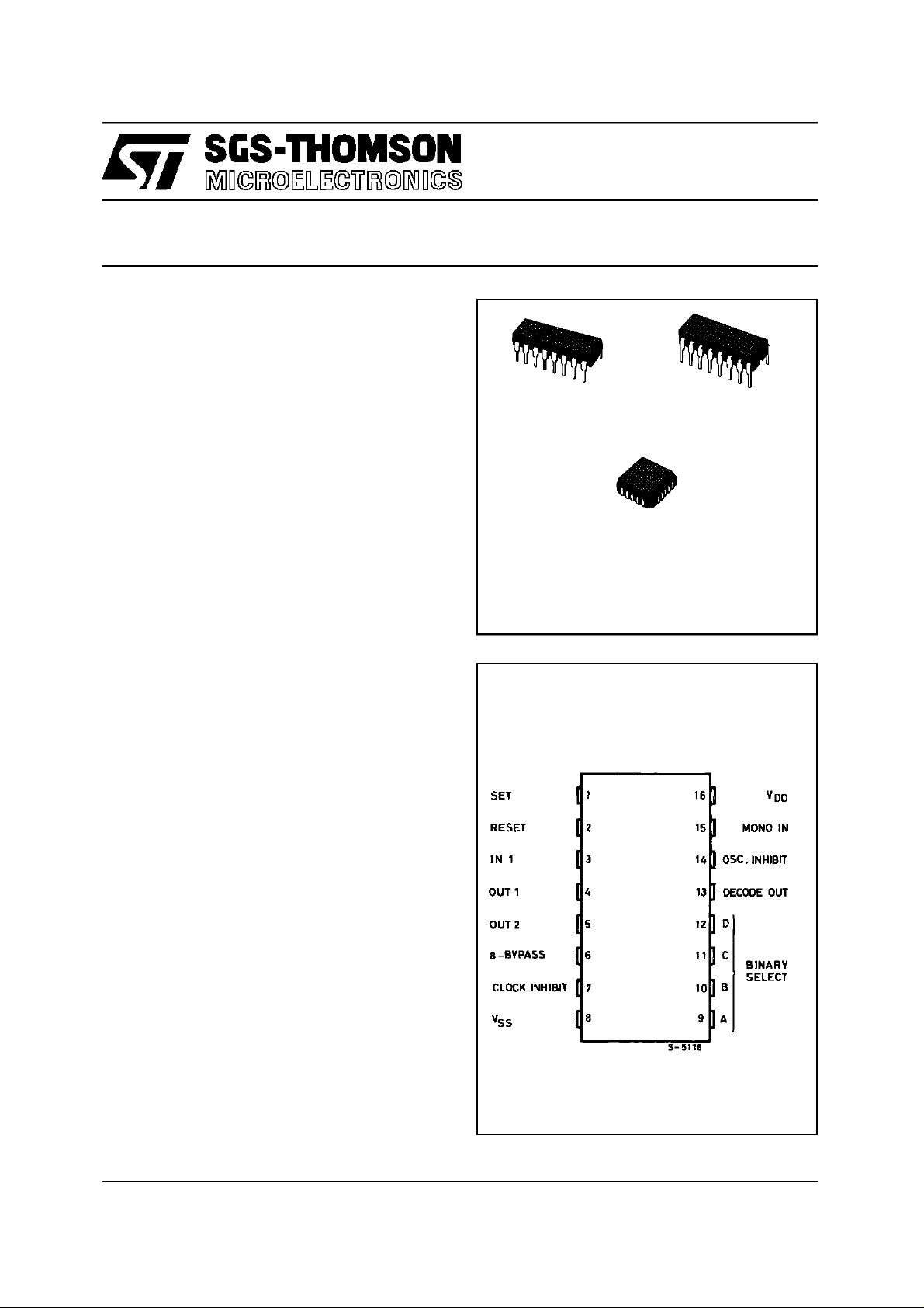
(Plastic Package)
(ChipCarrier)
ORDERCODES :
HCC 4536BF HCF4536BEY
PIN CONNECTIONS
(CeramicPackage)
C1
HCF4536BC1
F
DESCRIPT ION
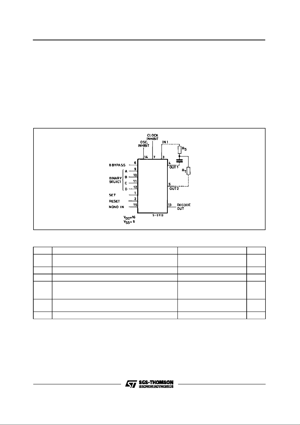
TheHCC4536B(extended temperature range) and
HCF4536B (intermediate temperature range) are
monolithic integrated circuits, available in 16-lead
dual in-line plastic or ceramic package. The
HCC/HCF4536B is a programmable timer consisting of 24 ripple-binary counter stages.Thesalient
featureof this device is its flexibility. The devicecan
count from 1 to 224or the first 8 stages can be bypassed to allow an output, selectable by a 4-bit code, from any oneof the remaining 16 stages. It can
be driven by an external clock or an RC oscillator
that canbe constructedusing on-chip components.
November1996
1/17
HCC/HCF4536B
InputIN1serves as either theexternal clockinputor
the input to the on-chip RC oscillator. OUT1 and
OUT2 are connection terminalsfor the external RC
components.Inaddition,anon-chipmonostablecircuit is provided to allow a variable pulse widthoutput. Various timing functionscan be achieved using
combinations of these capabilities. A logic 1 on the
8-BYPASS input enables a bypass of the first 8 stages and makes stage 9 the firstcounterstageof the
last16stages.Selection of1of16 outputsisaccomplished by the decoder andthe BCD inputs A, B, C
FUN CTIONAL DI AG R A M
and D. MONO IN is the timing input for the on-chip
monostable oscillator. Grounding of the MONO IN
terminalthrough a resistor of10KΩ or higher, disables the one-shot circuitand connects the decoder
directly to the DECODE OUT terminal. A resistorto
VDDand a capacitor to ground from the MONO IN
terminalenables theone-shot circuitand controls its
pulse width. A fast test mode is enabled by a logic
1 on 8-BYPASS, SET, and RESET. This mode divides the 24-stage counter into three 8-stagesections to facilitate a fast test sequence.
ABSOLUTE MAXIMUM RAT IN G S
Symbol Parameter Value Unit
V
* Supply Voltage : HCC Types
DD
V
Input Voltage – 0.5 to VDD+ 0.5 V
i
I
DC Input Current (any one input) ± 10 mA
I
P
T
T
Stresses abovethose listed under”Absolute MaximumRatings”may cause permanent damage tothe device. Thisisa stressrating onlyand
functionaloperation of the device at theseor any other conditions abovethose indicated intheoperational sectionsof thisspecification is not
implied.Exposure toabsolutemaximum ratingconditionsforexternal periods may affectdevice reliability.
* All voltages are withrespect to VSS(GND).
2/17
Total Power Dissipation (per package)
tot
Dissipation per Output Transistor
for Top= Full Package-temperature Range
Operating Temperature : HCC Types
op
Storage Temperature – 65 to + 150 °C
stg
HCF Types
HCF Types
– 0.5 to + 20
– 0.5 to + 18
200
100
– 55 to + 125
–40to+85
V
V
mW
mW
°C
°C
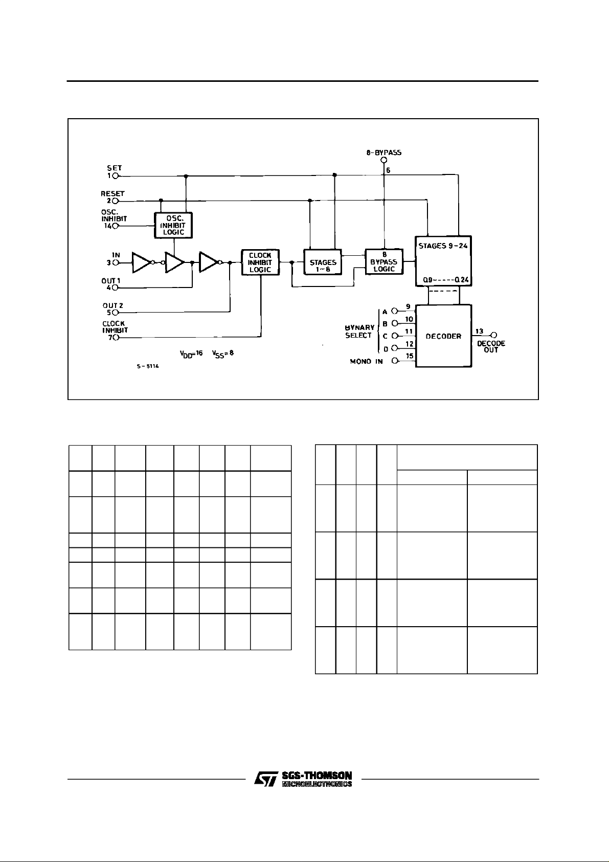
BLOCK DIAGRAM
HCC/HCF4536B
TRUTH TABLE
Clock
In 1 Set Reset
–
00 00
/
–
–
00 00
\
–
X1 0 0 0 0 1 1
X0 1 0 0 0 1 0
X0 0 1 0
00 0 0 X 0 1
10 0 0
0 = Low Level
Inh
Osc
Inh
–
–
/
Out1 Out2
–
/
–
–
\
–
–
\
–
–
\
–
–
/
–
–
/
–
Decode
Out
Change
Advance
to Next
State
Change
Change
Advance
to Next
State
No
No
No
DECO D E O UT SELECTIO N TABLE
Number o r Stage s
DCBA
0
0
0
0
0
0
1
0
0
1
0
0
0
1
0
0
1
0
0
1
1
0
1
1
1
0
0
1
0
0
1
0
1
1
0
1
0
1
1
0
1
1
1
1
1
1
1
1
0 = Low Level
0
1
0
1
0
1
0
1
0
1
0
1
0
1
0
1
In Divi d er C h ain
8-BYP ASS = 0 8-BY PASS = 1
9
10
11
12
13
14
15
16
17
18
19
20
21
22
23
24
1
2
3
4
5
6
7
8
9
10
11
12
13
14
15
16
3/17
HCC/HCF4536B
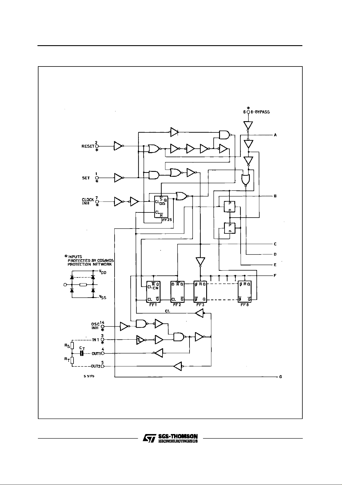
LOGI C DIAG RAM S (continued on next p age)
4/17
LOGI C DIAG RAM S (continued)
HCC/HCF4536B
5/17
HCC/HCF4536B
STATIC ELECTRICAL CHARACTERISTICS (over recommended operating conditions)
Test Conditions Valu e
Symbol Parameter
Quiescent
I
L
Current
HCC
Types
HCF
Types
V
OH
Output High
Voltage
V
OL
Output Low
Voltage
V
IH
Input High
Voltage
V
IL
Input Low
Voltage
I
OH
Output
Drive
Current
HCC
Types
HCF
Types
I
OL
Output
Sink
Current
HCC
Types
HCF
Types
I
IH,IIL
Input
Leakage
Current
HCC
Types
HCF
Types
C
Input Capacitance Any Input 5 7.5 pF
I
*T
=–55°C for HCC device: – 40°CforHCF device.
Low
*T
= + 125°C forHCCdevice : + 85°C for HCF device.
High
TheNoiseMargin for both ”1” and ”0” levelis: 1V min.with VDD=5V , 2Vmin. with VDD= 10V, 2.5 V min.with VDD=15V.
V
V
O
|IO|V
I
(V) (V) (µA) (V)
DD
T
* 25°CT
Low
High
Min. M ax. Min. Typ. Max. Min. Max.
0/ 5 5 5 0.04 5 150
0/10 10 10 0.04 10 300
0/15 15 20 0.04 20 600
0/20 20 100 0.08 100 3000
0/ 5 5 20 0.04 20 150
0/10 10 40 0.04 40 300
0/15 15 80 0.04 80 600
0/ 5 < 1 5 4.95 4.95 4.95
0/10 < 1 10 9.95 9.95 9.95
0/15 < 1 15 14.95 14.95 14.95
5/0 < 1 5 0.05 0.05 0.05
10/0 < 1 10 0.05 0.05 0.05
15/0 < 1 15 0.05 0.05 0.05
0.5/4.5 < 1 5 3.5 3.5 3.5
1/9 < 1 10 7 7 7
1.5/13.5 < 1 15 11 11 11
4.5/0.5 < 1 5 1.5 1.5 1.5
9/1 < 1 10 3 3 3
13.5/1.5 < 1 15 4 4 4
0/ 5 2.5 5 – 2 – 1.6 – 3.2 – 1.15
0/ 5 4.6 5 – 0.64 – 0.51 – 1 – 0.36
0/10 9.5 10 – 1.6 – 1.3 – 2.6 – 0.9
0/15 13.5 15 – 4.2 – 3.4 – 6.8 – 2.4
0/ 5 2.5 5 – 1.53 – 1.36 – 3.2 – 1.1
0/ 5 4.6 5 – 0.52 – 0.44 – 1 – 0.36
0/10 9.5 10 – 1.3 – 1.1 – 2.6 – 0.9
0/15 13.5 15 – 3.6 – 3.0 – 6.8 – 2.4
0/ 5 0.4 5 0.64 0.51 1 0.36
0/10 0.5 10 1.6 1.3 2.6 0.9
0/15 1.5 15 4.2 3.4 6.8 2.4
0/ 5 0.4 5 0.52 0.44 1 0.36
0/10 0.5 10 1.3 1.1 2.6 0.9
0/15 1.5 15 3.6 3.0 6.8 2.4
0/18
18
± 0.1 ±10
–5
± 0.1 ± 1
Any Input
0/15
15 ± 0.3 ±10
–5
± 0.3 ± 1
Unit
*
µA
V
V
V
V
mA
mA
µA
6/17

HCC/HCF4536B
DYNAMIC ELECTRICAL CHARACTERISTICS (T
=25oC, CL=50pF,RL= 200 KΩ,
amb
typic al temperat ure coefficent for all VDDvalues is 03 %/oC, all input ris e and f all t i mes = 20 ns)
Symbol Parameter
t
t
PLH
PHL
Propagation Delay Time
Clock to Q1, 8-bypass High
Clock to Q1, 8-bypass Low 5 2.5 5
Clock to Q16 5 4 8
Qnto Q
n+1
t
t
t
t
PLH
PHL
Propagation Delay Time 5 300 600
Reset to Qn 5 3 6
Transition Time 5 100 200
TLH
THL
Pulse Width
t
W
Clock
Set 5 200 400
Reset 5 3 6
Recovery Time
Set
Reset 5 3.5 7
t
f
Clock Input Rise or Fall Time 5
r,tf
Maximum Clock Input Frequency 0.5 1
CL
Test Conditions Value
(V) Min. Typ. Max.
V
DD
512
10 0.5 1
15 0.35 0.7
10 0.8 1.6
15 0.6 1.2
10 1.5 3
15 1 2
5 150 300
10 75 150
15 50 100
10 125 250
15 80 160
10 1 2
15 0.75 1.5
10 50 100
15 40 80
5 200 400
10 75 150
15 50 100
10 100 200
15 60 120
10 1 2
15 0.75 1.5
5 2.5 5
10 1 2
15 0.6 1.6
10 1.5 3
15 1 2
10
Unlimted µs
15
10 1.5 3
15 2.5 5
Unit
µs
µs
µs
ns
ns
µs
ns
ns
ns
µs
µs
µs
MHz
7/17

HCC/HCF4536B
OutputLow (sink) Current Characteristics. Output High (source)Current Characteristics.
Typical Transition Time vs. Load Capacitance. TypicalPropagation Delay Time vs. Load Capacit-
ance (clock to Q1, 8 Bypasshigh).
TypicalPropagation Delay Time vs.Load Capacitance(Clock to Q1,8 Bypass low).
8/17
TypicalPropagation DelayTime vs. Load Capacitance(Clock to Q16, 8 Bypass high).

HCC/HCF4536B
TypicalPropagation Delay Time vs.Load Capacitance(QNtoQ
N+1
).
TypicalRC OscillatorFrequency Deviation vs.
Time Constant Resistance and Capacitance.
TypicalRC OscillatorFrequency Deviationvs.
Supply Voltage.
TypicalRC OscillatorFrequency Deviationvs. Ambient Temperature (RS=0).
TypicalRC OscillatorFrequency Deviation vs. AmbientTemperature (RS= 120KΩ).
TypicalPulse Width vs. External Capacitance
(VDD= 5V).
9/17

HCC/HCF4536B
Typical Pulse Widthvs. External Capacitance
(VDD= 10V).
TypicalDynamic Power Dissipation vs. Input
Pulse Frequency.
Typical Pulse Width vs. External Capacitance
(VDD= 15V).
TYPICAL APPLI CA TI ONS
Time InternalConfiguration Using External Clock
; Setand Clock Inhibit Functions.
10/17
TimeInternal Configuration Using External Clock
; Resetand Output Monostable to Achieve a
Pulse Output.

TYPICAL APPLI CA TI ONS ( Continued)
HCC/HCF4536B
Time Internal Configuration UsingOnchip RCOscillator and Reset Input to Initiate TimeInterval.
Application Showing Use of 4098B and 4536B to
get DecodePulse 8 ClockPulses after Reset
TIMING DIAGRAM
11/17

HCC/HCF4536B
Functional Tes t Sequence
Inputs Outputs Comments
In 1 Se t R eset 8- Bypass
101 1 0
111 1 0
0 1 1 1 0 First ”1” to ”0” Transition of Clock
1
0
–
–
0 1 1 1 1 The 255 ”1” to ”0” Transition
000 0 1
100 0 1 In
0 0 0 0 0 Counter Ripples from an all ”1” state to an all ”0”
11 1
Decade Out
Q 1 Thru Q 24
All 24 step s a re in rese t mo de.
Counter is in three 8-stage section in parallel
mode.
255 ”1” to ”0” transitions are clocked in the
counter.
Counter converted back to 24 stages in series
mode.
Set and Reset must be connected together and
simultaneoulsy go from ”1” to ”0”.
switches to a ”1”.
1
state.
FUNCTIONAL TEST SEQUENCE
TestFunction hasbeenincluded forthereduction of
test timerequired to exerciseall 24 counterstages.
This test function divides the counter into three 8stage section and255 counts are loadedin eachof
the 8-stagesectionsin parallel. Allflip-flopsarenow
TEST CIRCUITS
at a ”1”. The counter is now returned to the normal
24-steps in series configuration. One more pulse is
enteredintoIn1whichwillcausethecounter toripple
from an all ”1” stateto an all ”0” state.
Input Voltage.QuiescentDevice Current.
12/17

TEST CIRCUITS (continued)
HCC/HCF4536B
Input Leakage Current.
SwitchingTime.
Dynamic Power Dissipation.
Input Waveforms for Switching-Time.
Functional.
13/17

HCC/HCF4536B
Plastic DIP16 (0.25) MECHANICAL DATA
DIM.
MIN. TYP. MAX. MIN. TYP. MAX.
a1 0.51 0.020
B 0.77 1.65 0.030 0.065
b 0.5 0.020
b1 0.25 0.010
D 20 0.787
E 8.5 0.335
e 2.54 0.100
e3 17.78 0.700
F 7.1 0.280
I 5.1 0.201
L 3.3 0.130
Z 1.27 0.050
mm inch
14/17
P001C

Ceramic DIP16/1 MECHANICAL DATA
HCC/HCF4536B
DIM.
MIN. TYP. MAX. MIN. TYP. MAX.
A 20 0.787
B 7 0.276
D 3.3 0.130
E 0.38 0.015
e3 17.78 0.700
F 2.29 2.79 0.090 0.110
G 0.4 0.55 0.016 0.022
H 1.17 1.52 0.046 0.060
L 0.22 0.31 0.009 0.012
M 0.51 1.27 0.020 0.050
N 10.3 0.406
P 7.8 8.05 0.307 0.317
Q 5.08 0.200
mm inch
P053D
15/17

HCC/HCF4536B
PLCC20 MECHANICAL DATA
DIM.
MIN. TYP. MAX. MIN. TYP. MAX.
A 9.78 10.03 0.385 0.395
B 8.89 9.04 0.350 0.356
D 4.2 4.57 0.165 0.180
d1 2.54 0.100
d2 0.56 0.022
E 7.37 8.38 0.290 0.330
e 1.27 0.050
e3 5.08 0.200
F 0.38 0.015
G 0.101 0.004
M 1.27 0.050
M1 1.14 0.045
mm inch
16/17
P027A

HCC/HCF4536B
Information furnished is believed to be accurate and reliable. However, SGS-THOMSON Microelectronics assumes no responsability for the
consequences of use of such information nor for any infringementof patents or other rights of third parties which may results from its use. No
licenseis granted by implication orotherwise under any patentor patent rights of SGS-THOMSON Microelectronics. Specificationsmentioned
in thispublication are subject tochange withoutnotice. Thispublicationsupersedes andreplacesall information previously supplied.
SGS-THOMSONMicroelectronics products are not authorized for use as criticalcomponents in lifesupport devices or systemswithoutexpress
writtenapproval ofSGS-THOMSONMicroelectonics.
1996SGS-THOMSONMicroelectronics - Printedin Italy- All RightsReserved
Australia- Brazil - Canada - China - France- Germany - Hong Kong- Italy - Japan- Korea- Malaysia - Malta- Morocco- The Netherlands -
Singapore - Spain- Sweden- Switzerland- Taiwan - Thailand- UnitedKingdom - U.S.A
SGS-THOMSONMicroelectronics GROUPOFCOMPANIES
.
17/17
 Loading...