


DUAL 4-CHANNEL OR SINGLE 8-CHANNEL
.DATA PATHSARE BIDIRECTIONAL
.10 MHz OPERATION (typical)
.3-STATE OUTPUTS
.”ON” RESISTANCE 125 W TYPICAL @ 15V
.SUPPLYVOLTAGE RANGE = 3Vdc TO18Vdc
HCC4529B
HCF4529B
ANALOG DATASELECTOR
DESCRIPTION
The HCC4529B (extended temperataure range)
and HCF4529b (intermediate temperature range)
are monolithic integrated circuits available in 16leaddualinlineplasticorceramicpackageandplastic micropackage.
The HCC/HCF4529b isa DUAL4-CHANNEL or 8CHANNELdevice.Oneof thetwo possiblefunctions can be selected by aproper input coding. For the
single 8-bit mode Z and W output must be tied
together.
HCC/HCF4529B is suitable for digital as well as
analogue applications, including 1 of 4 and 1 of 8
dataselectorfunctions.Dualbinaryto1 of4 orsingle
binary to 1 of 8 decoder applications can be implemented because the deviceallow analogue and
bidirectional operation.
EY
(PlasticPackage)
M1
(MicroPackage)
ORDER CODES :
HCC4 529BF HCF4529BM1
HCF4529BEY HCF4529BC1
PIN CONNECTIONS
(CeramicPackage)
(Chip Carrier)
F
C1
September 1988
1/10

HCC/HCF4529B
ABSOLU TE MAXIMU M RAT ING
Symbol Parameter Value Unit
V
* Supply Voltage: HCC Types
DD
HCF Types
V
P
Input Voltage -0.5 to VDD+ 0.5 V
i
I
DC Input Current (any one input) ± 10 mA
I
Total Power Dissipation (per package)
tot
Dissipation per Output Transistor
for Top = Full Package Temperature Range
T
Operating Temperature: HCC Types
op
HCF Types
T
Stressesabove thoselistedunder ”Absolute MaximumRatings”maycausepermanent damage to thedevice. Thisisa stressratingonly and functional
operation of the device atthese oranyother conditions above thoseindicated in theoperational sections of thisspecification isnot implied.Exposure
to absolute maximum ratingconditions for external periods may affectdevice reliability.
* All voltagevalues are referredto VSSpinvoltage.
Storage Temperature -65 to +150
stg
-0.5 to +20
-0.5 to +18
200
100
-55 to +125
-40 to +85
V
V
mW
mW
o
C
o
C
o
C
TRUTH TABLE
STXST
1100X0Y0
1101X1Y1
1110X2Y2
1111X3Y3
1000 X0
1001 X1
1010 X2
1011 X3
0100 Y0
0101 Y1
B A Z W MODE
Y
Dual
4-Channel
Mode
2 Outputs
Single
8-Channel
Mode
1 Output
(Z and W
tied
together)
FUNCTIONAL DIAGRAM
0110 Y2
0111 Y3
0 0 X X High
Impedance
X = Don’t care
RECO MM ENDED OPERATI N G CONDI TI O NS
Symbol Parameter Value Unit
V
V
T
Supply Voltage: HCC Types
DD
HCF Types
Input Voltage 0 to V
I
Operating Temperature: HCC Types
op
HCF Types
3to18
3to15
DD
-55 to +125
-40 to +85
V
V
V
o
C
o
C
2/10
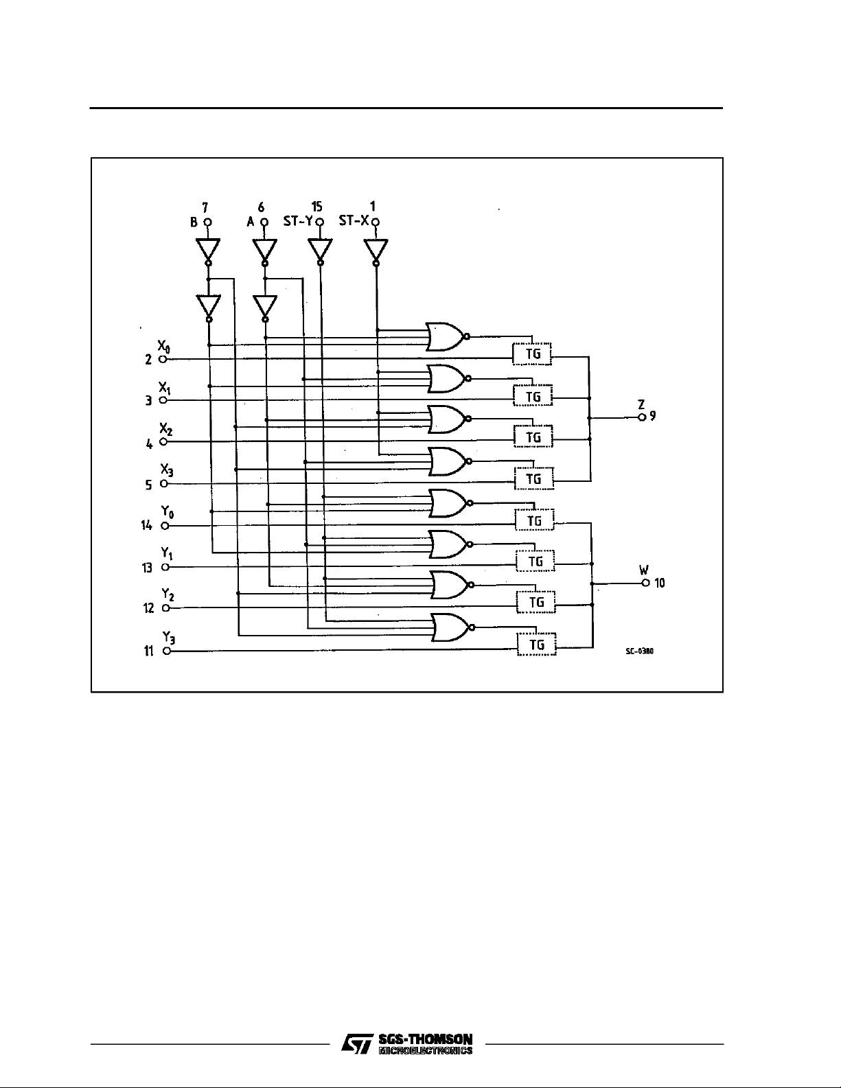
BLOCK DIAGRAM
HCC/HCF4529B
3/10

HCC/HCF4529B
STATI C E LE CT RIC AL CHAR ACTER I STI CS (ov er rec ommended opera t ing conditio ns)
Test Conditios Value
Symbol Parameter
Quiescent
I
L
Current
HCC
Types
V
(V)
IS
V
(V)
SS
V
(V)
T
DD
*25
LOW
Min. Max. Min. Typ. Max. Min. Max.
5 5 0.04 5 150
10 10 0.04 10 300
15 20 0.04 20 600
o
CT
20 100 0.08 100 3000
HCF
Types
5 20 0.04 20 150
10 40 0.04 40 300
15 80 0.04 80 600
SWITCH
ON Resistance
HCC
Types
0 ≤ V
≤ V
DD
I
0
5 880 470 1050 1200
10 310 180 400 580
15 220 125 280 400
HCC
Types
0 ≤ V
≤ V
DD
I
0
5 880 470 1050 1200
10 330 180 400 520
15 230 125 280 360
∆ON Resistance ∆R
(Between any 2
channels)
OFF
Channel
Leakage
Current
Any
Channel
OFF
All Channel
OFF
(common
ON
HCC
Types
HCC
Types
0
0 18 100 ±0.1 100 1000 nA
0 18 100 ±0.1 100 1000 nA
510
10 10
15 5
OUT/IN)
Any
Channel
OFF
HCC
Types
0 15 300 ±0.1 300 1000 nA
All Channel
OFF
(common
HCC
Types
0 15 300 ±0.1 300 1000 nA
OUT/IN)
CONTROL (Address or Inhibit)
V
V
IL
IH
Input Low
Voltage
Input High
Voltage
=V
thru
1KΩ
DD
RL=1KΩ
to V
SS
IIS<2µA
(On All
OFF
Channels)
5 1.5 1.5 1.5
10 3 3 3
15 4 4 4
5 3.5 3.5 3.5
10 7 7 7
15 11 11 11
I
IH,IIL
Input
Leakage
Current
C
*T
LOW
*T
HIGH
TheNoiseMargin for both ”1” and ”0” level is: 1V min. withVDD=5V, 2V min.with VDD=10 V,2.5Vmin.withVDD=15V
Input Capacitance Any Input 5 7.5 pF
I
=-55oCforHCCdevice: -40oC for HCF device.
=+125oCforHCC device:+85oC for HCF device.
HCC
Types
HCF
Types
V
= 0/18V 18 ±0.1 ±10-3±0.1 ±1
I
V
= 0/15V 15 ±0.3 ±10-3±0.3 ±1
I
HIGH
Unit
*
µA
Ω
Ω
V
V
µA
4/10

HCC/HCF4529B
DYNAMIC ELECTRICAL CHARACTERISTICS (T
=25oC, CL=50pF,RL= 200 KΩ,
amb
typic al temper at ure coeffi c ent f or all VDDvalues is 03 %/oC, a ll input rise and fall t im es = 20 ns)
Symbol Parameter
t
t
t
t
PLH
PHL
PLH
PHL
Vinto V
Propagation Delay Time
out
(CL= 50pF, RL=1KΩ)
Propagation Delay Time, Control to Output,
Vin = VDDor V
SS
(Vin≤ 10 Vdc, CL= 50pF, RL=1KΩ)
Crosstalk, Control to Output
= 50pF, RL=1KΩ,R
(C
L
Maximum Control Input Pulse Frequency
= 50pF, RL=1KΩ)
(C
L
Sine Wave (Distortion) (V
in
Centred @ 0.0 Vdc, RL=10KΩ, f = 1 KHz)
BW Bandwidth (-3 dB) (V
= 1.77 Vdc RMS
in
Centred @ 0.0 Vdc)
(RL=1KΩ)
(RL= 10KΩ)
(RL= 100KΩ)
(R
=1MΩ)
L
Feedthrough and Crosstalk
Log
10
=1KΩ)
V
out
=−50
V
in
dB
(R
20
L
(RL= 10KΩ)
(RL= 100KΩ)
(RL=1MΩ)
=10KΩ)
out
= 1.77 Vdc RMS
Test Conditions Value
V
(V) VDD(V) Min. Typ. Max.
SS
0 5 20 40
10 10 20
15 8 15
0 5 200 400
10 80 160
15 50 120
05 5
10 5
15 5
05 5
10 10
15 12
-5 5 0.36
-5 5
35
28
27
26
-5 5
850
100
12
1.5
Unit
ns
ns
mV
MHz
%
MHz
KHz
5/10

HCC/HCF4529B
Plastic DIP16 (0.25) MECHANICAL DATA
DIM.
MIN. TYP. MAX. MIN. TYP. MAX.
a1 0.51 0.020
B 0.77 1.65 0.030 0.065
b 0.5 0.020
b1 0.25 0.010
D 20 0.787
E 8.5 0.335
e 2.54 0.100
e3 17.78 0.700
F 7.1 0.280
I 5.1 0.201
L 3.3 0.130
Z 1.27 0.050
mm inch
6/10
P001C

Ceramic DIP16/1 MECHANICAL DATA
HCC/HCF4529B
DIM.
MIN. TYP. MAX. MIN. TYP. MAX.
A 20 0.787
B 7 0.276
D 3.3 0.130
E 0.38 0.015
e3 17.78 0.700
F 2.29 2.79 0.090 0.110
G 0.4 0.55 0.016 0.022
H 1.17 1.52 0.046 0.060
L 0.22 0.31 0.009 0.012
M 0.51 1.27 0.020 0.050
N 10.3 0.406
P 7.8 8.05 0.307 0.317
Q 5.08 0.200
mm inch
P053D
7/10

HCC/HCF4529B
SO16 (Narrow) MECHANICAL DATA
DIM.
MIN. TYP. MAX. MIN. TYP. MAX.
A 1.75 0.068
a1 0.1 0.2 0.004 0.007
a2 1.65 0.064
b 0.35 0.46 0.013 0.018
b1 0.19 0.25 0.007 0.010
C 0.5 0.019
c1 45° (typ.)
D 9.8 10 0.385 0.393
E 5.8 6.2 0.228 0.244
e 1.27 0.050
e3 8.89 0.350
F 3.8 4.0 0.149 0.157
G 4.6 5.3 0.181 0.208
L 0.5 1.27 0.019 0.050
M 0.62 0.024
S8°(max.)
mm inch
8/10
P013H

PLCC20 MECHANICAL DATA
HCC/HCF4529B
DIM.
MIN. TYP. MAX. MIN. TYP. MAX.
A 9.78 10.03 0.385 0.395
B 8.89 9.04 0.350 0.356
D 4.2 4.57 0.165 0.180
d1 2.54 0.100
d2 0.56 0.022
E 7.37 8.38 0.290 0.330
e 1.27 0.050
e3 5.08 0.200
F 0.38 0.015
G 0.101 0.004
M 1.27 0.050
M1 1.14 0.045
mm inch
P027A
9/10

HCC/HCF4529B
Information furnished is believed to be accurate and reliable. However, SGS-THOMSON Microelectronics assumes no responsability forthe
consequences of use of such information nor for any infringement of patents or other rights of third parties which may results from its use. No
license is granted byimplication or otherwise underany patentor patent rights ofSGS-THOMSON Microelectronics.Specificationsmentioned
in this publication aresubject to changewithout notice. This publication supersedes and replaces all information previously supplied.
SGS-THOMSON Microelectronicsproducts are not authorized foruse ascritical componentsinlife supportdevices or systemswithoutexpress
written approval of SGS-THOMSON Microelectonics.
1994 SGS-THOMSON Microelectronics- All RightsReserved
Australia - Brazil - France - Germany - Hong Kong - Italy - Japan - Korea - Malaysia - Malta - Morocco - The Netherlands-
Singapore -Spain - Sweden - Switzerland - Taiwan - Thailand - UnitedKingdom - U.S.A
SGS-THOMSON Microelectronics GROUP OF COMPANIES
10/10
 Loading...