


HCC/ HC F4 518B DUAL BCD U P -CO UNT ER
HCC/ HC F4 520B DUA L BINA RY UP-
COUNTER
.MEDIUM-SPEED OPERATION – 6MHz TYP.
CLOCKFREQUENCY AT 10V
.POSITIVE - OR NEGATIVE - EDGETRIGGER-
ING
.SYNCHRONOUSINTERNAL CARRYPROPA-
GATION
.QUIESCENT CURRENT SPECIFIED TO 20V
FOR HCC DEVICE
.5V, 10V,AND 15VPARAMETRIC RATINGS
.INPUT CURRENTOF100nAAT 18V AND25°C
FOR HCC DEVICE
.100% TESTEDFOR QUIESCENTCURRENT
.MEETSALLREQUIREMENTSOFJEDECTEN-
TATIVESTANDARDN°13A,”STANDARD SPECIFICATIONS FOR DESCRIPTION OF ”B”
SERIESCMOS DEVICES”
HCC/HCF4518B
HCC/HCF4520B
DUAL UP-COUNTERS
EY
(Plastic Package)F(CeramicFritSeal Package)
M1
(MicroPackage)
ORDER CODES :
HCC45XXBF HCF45XXBM1
HCF45XXBEY HCF45XXBC1
(Plastic ChipCarrier)
C1
DESCRIPTI ON
The HCC4518B/4520B (extended temperature
range) and HCF4518B/4520B (intermediate tem-
perature range) are monolithic integrated circuits,
available in 16-lead dual in-line plastic or ceramic
package and plastic micro package. The
HCC/HCF4518B Dual BCD Up Counter and
HCC/HCF4520BDualBinaryUpCountereachcon-
sist of two identical, internally synchronous 4-stage
counters. The counter stages are D-type flip-flops
having interchangeable Clock and Enable lines for
incrementing on either the positive-going or negative-going transition. For single-unit operation the
Enable input is maintained ”high” and the counter
advances on each positive-going transition of the
Clock. The counters are cleared by high levels on
their Reset lines. The counter can be cascaded in
the ripple mode by connecting Q4 to the enable
inputofthesubsequent counterwhiletheclockinput
of the latter isheld low.
PIN CONNECTIONS
June1989
1/14

HCC/HCF4518B/4520B
FUN CTIONAL DIAGRA M
ABSOLUTE M AXI MUM RATI N GS
Symbol Parameter Value Unit
* Supply Voltage :HCC Types
V
DD
HCF Types
V
Input Voltage – 0.5 to VDD+ 0.5 V
i
I
DC Input Current (any one input) ± 10 mA
I
P
Total Power Dissipation (per package)
tot
Dissipation per Output Transistor
for T
T
Operating Temperature : HCC Types
op
= Full Package-temperature Range
op
HCF Types
T
Stresses above those listed under ”Absolute Maximum Ratings” may cause permanent damage to the device. This is a stress
rating only and functional operation of the device at these or any other conditions above those indicated in the operational sections
of this specification is not implied. Exposure to absolute maximum rating conditions for external periods may affect device reliability.
* All voltage values are referred to VSSpin voltage.
Storage Temperature – 65 to + 150 °C
stg
– 0.5 to + 20
– 0.5 to + 18
200
100
– 55 to + 125
–40to+85
V
V
mW
mW
°C
°C
RECOMMENDED OPERATING CONDITIONS
Symbol Parameter Value Unit
V
T
2/14
Supply Voltage : HCC Types
DD
HCF Types
V
Input Voltage 0 to V
I
Operating Temperature : HCC Types
op
HCF Types
3to18
3to15
DD
– 55 to + 125
–40to+85
V
V
V
°C
°C

LOGI C DIAG RAM S (for one of two identical counter )
DecadeCounter for4518B.
HCC/HCF4518B/4520B
BinaryCounterfor 4520B.
3/14
HCC/HCF4518B/4520B
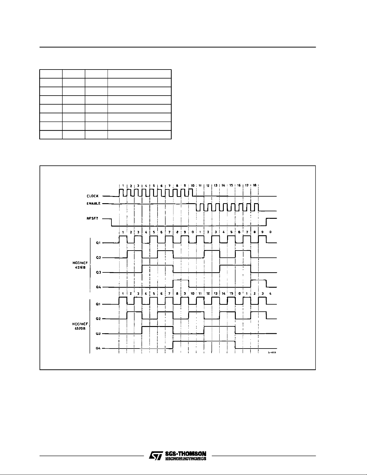
TRUTH TABLE
Clock Ena b le Re s e t Action
–
/
–
0
–
\
–
X
–
/
–
1
X X 1 Q1ThruQ4=0
X = Don’t Care Logic 1 = High State Logic 0 = Low
TIM ING DIAG R AM
1 0 Increment Counter
–
\
–
X 0 No Change
–
/
–
0 0 No Change
–
\
–
0 Increment Counter
0 No Change
0 No Change
4/14
HCC/HCF4518B/4520B
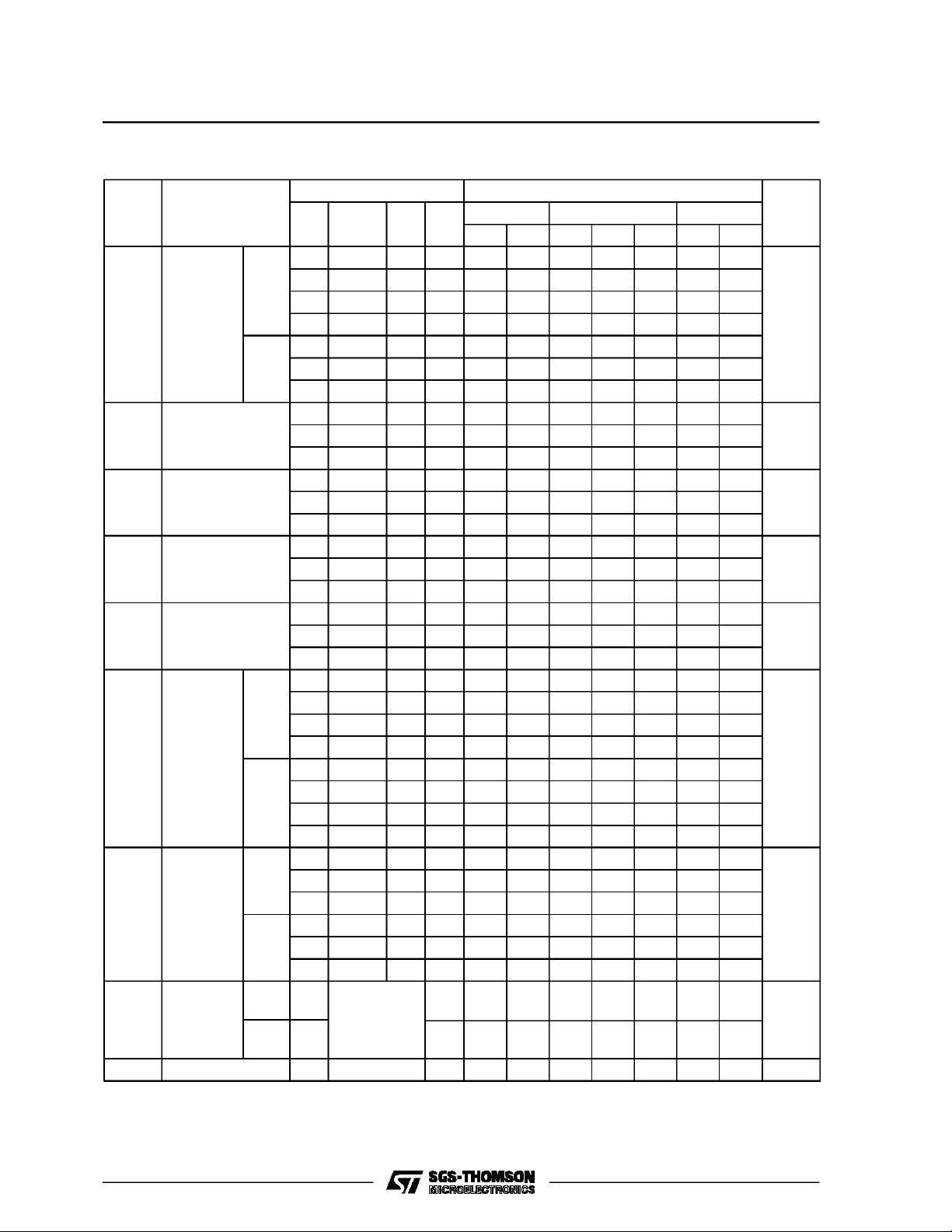
STATIC ELECTRICAL CHARACTERISTICS (overrecommended operating conditions)
Test Conditions Value
Symbol Parame te r
(V) (V) (µA) (V)
I
L
Quiescent
Current
HCC
Types
0/ 5 5 5 0.04 5 150
0/10 10 10 0.04 10 300
0/15 15 20 0.04 20 600
0/20 20 100 0.08 100 3000
0/ 5 5 20 0.04 20 150
HCF
Types
0/10 10 40 0.04 40 300
0/15 15 80 0.04 80 600
V
OH
Output High
Voltage
0/ 5 < 1 5 4.95 4.95 4.95
0/10 < 1 10 9.95 9.95 9.95
0/15 < 1 15 14.95 14.95 14.95
V
OL
Output Low
Voltage
5/0 < 1 5 0.05 0.05 0.05
10/0 < 1 10 0.05 0.05 0.05
15/0 < 1 15 0.05 0.05 0.05
V
IH
Input High
Voltage
V
IL
Input Low
Voltage
I
OH
Output
Drive
Current
HCC
Types
0/ 5 2.5 5 – 2 – 1.6 – 3.2 – 1.15
0/ 5 4.6 5 – 0.64 – 0.51 – 1 – 0.36
0/10 9.5 10 – 1.6 – 1.3 – 2.6 – 0.9
0/15 13.5 15 – 4.2 – 3.4 – 6.8 – 2.4
0/ 5 2.5 5 – 1.53 – 1.36 – 3.2 – 1.1
HCF
Types
0/ 5 4.6 5 – 0.52 – 0.44 – 1 – 0.36
0/10 9.5 10 – 1.3 – 1.1 – 2.6 – 0.9
0/15 13.5 15 – 3.6 – 3.0 – 6.8 – 2.4
I
OL
Output
Sink
Current
HCC
Types
0/ 5 0.4 5 0.64 0.51 1 0.36
0/10 0.5 10 1.6 1.3 2.6 0.9
0/15 1.5 15 4.2 3.4 6.8 2.4
0/ 5 0.4 5 0.52 0.44 1 0.36
HCF
Types
0/10 0.5 10 1.3 1.1 2.6 0.9
0/15 1.5 15 3.6 3.0 6.8 2.4
I
IH,IIL
*T
Low
*T
High
The Noise Margin for both ”1” and ”0” level is : 1V min. with VDD= 5V, 2V min. with VDD= 10V, 2.5V min. with VDD= 15V.
Input
Leakage
Current
C
Input Capacitance Any Input 5 7.5 pF
I
=–55°CforHCC device : – 40°CforHCF device.
= + 125°CforHCC device : + 85°CforHCF device.
HCC
Types
HCF
Types
0/18
0/15
V
V
I
O
|IO|V
DD
T
* 25°CT
Low
Min. Max. Min. Typ. Max. Min. Max.
0.5/4.5 < 1 5 3.5 3.5 3.5
1/9 < 1 10 7 7 7
1.5/13.5 < 1 15 11 11 11
4.5/0.5 < 1 5 1.5 1.5 1.5
9/1 < 1 10 3 3 3
13.5/1.5 < 1 15 4 4 4
–5
18 ± 0.1 ±10
± 0.1 ± 1
Any Input
15 ± 0.3 ±10
–5
± 0.3 ± 1
High
*
Unit
µA
V
V
V
V
mA
mA
µA
5/14

HCC/HCF4518B/4520B
DYNAMIC ELECTRICAL CHARACTERISTICS (T
=25°C,CL= 50pF, RL=200kΩ,
amb
typicaltemperature coefficient for allVDD=0.3%/°C values,all input rise andfall time= 20ns)
Symbol Parameter
t
,
PLH
t
PHL
t
PLH
t
PHL
t
TLH,tTHL
t
t
t
t
f
max
t
Propagation Delay Time
(clock or enable to output)
,
Propagation Delay Time
,
(reset to output)
Transition Time 5 100 200
Clock Pulse Width 5 200 100
W
Reset Pulse Width 5 250 125
W
Enable Pulse Width 5 400 200
W
,
Clock or Enable Rise and Fall
r
t
Time
f
Maximum Clock Frequency 5 1.5 3
,
Clock Input Rise or Fall Time 5 15
r
t
f
Test Conditions Valu e
V
(V) Min. Typ. Max.
DD
5280560
10 115 230
15 80 160
5330650
10 130 225
15 90 170
10 50 100
15 40 80
10 100 50
15 70 35
10 110 55
15 80 40
10 200 100
15 140 70
515
10 15
15 5
10 3 6
15 4 8
10 5
15 5
Unit
ns
ns
ns
ns
ns
ns
µs
MHz
µs
6/14

HCC/HCF4518B/4520B
TypicalOutput Low (sink) Current Characteristics.
Mini-
TypicalOutput High (source) Current Characteristics.
mum Output Low (sink) Current Characteristics.
Minimum output High(source) Current Characteristics.
TypicalPropagation Delay vs. LoadCapacitance,
Reset to output.
TypicalPropagation Delay Time vs.Load Capacitance, Clock or Enable toOutput.
7/14

HCC/HCF4518B/4520B
TypicalTransitionTime vs.load Capacitance. Typical Maximum-clockFrequency vs, Supply
Voltage.
TypicalPower Dissipation/Counter vs.Frequency.
TYPICAL APPLI CA TI O NS
RIPPLECASCADINGOF FOURCOUNTERS WITHPOSITIVE-EDGE TRIGGERING.
8/14

HCC/HCF4518B/4520B
SYNCHRONOUSCASCADING OF FOUR BINARY COUNTERS WITHNEGATIVE-EDGE TRIGGERING.
TEST CIRCUITS
QuiescentDevice Current. Noise Immunity.
Input Leakage Current. DynamicPower Dissipation.
9/14

HCC/HCF4518B/4520B
Plastic DIP16 (0.25) MECHANICAL DATA
DIM.
MIN. TYP. MAX. MIN. TYP. MAX.
a1 0.51 0.020
B 0.77 1.65 0.030 0.065
b 0.5 0.020
b1 0.25 0.010
D 20 0.787
E 8.5 0.335
e 2.54 0.100
e3 17.78 0.700
F 7.1 0.280
I 5.1 0.201
L 3.3 0.130
Z 1.27 0.050
mm inch
10/14
P001C

HCC/HCF4518B/4520B
Ceramic DIP16/1 MECHANICAL DATA
DIM.
MIN. TYP. MAX. MIN. TYP. MAX.
A 20 0.787
B 7 0.276
D 3.3 0.130
E 0.38 0.015
e3 17.78 0.700
F 2.29 2.79 0.090 0.110
G 0.4 0.55 0.016 0.022
H 1.17 1.52 0.046 0.060
L 0.22 0.31 0.009 0.012
M 0.51 1.27 0.020 0.050
N 10.3 0.406
P 7.8 8.05 0.307 0.317
Q 5.08 0.200
mm inch
P053D
11/14

HCC/HCF4518B/4520B
SO16 (Narrow) MECHANICAL DATA
DIM.
MIN. TYP. MAX. MIN. TYP. MAX.
A 1.75 0.068
a1 0.1 0.2 0.004 0.007
a2 1.65 0.064
b 0.35 0.46 0.013 0.018
b1 0.19 0.25 0.007 0.010
C 0.5 0.019
c1 45° (typ.)
D 9.8 10 0.385 0.393
E 5.8 6.2 0.228 0.244
e 1.27 0.050
e3 8.89 0.350
F 3.8 4.0 0.149 0.157
G 4.6 5.3 0.181 0.208
L 0.5 1.27 0.019 0.050
M 0.62 0.024
S8°(max.)
mm inch
12/14
P013H

PLCC20 MECHANICAL DATA
HCC/HCF4518B/4520B
DIM.
MIN. TYP. MAX. MIN. TYP. MAX.
A 9.78 10.03 0.385 0.395
B 8.89 9.04 0.350 0.356
D 4.2 4.57 0.165 0.180
d1 2.54 0.100
d2 0.56 0.022
E 7.37 8.38 0.290 0.330
e 1.27 0.050
e3 5.08 0.200
F 0.38 0.015
G 0.101 0.004
M 1.27 0.050
M1 1.14 0.045
mm inch
P027A
13/14

HCC/HCF4518B/4520B
Information furnished isbelieved tobe accurate and reliable. However, SGS-THOMSON Microelectronics assumes no responsability for the
consequences of use of suchinformation nor for any infringementof patents or other rightsof third partieswhich may resultsfrom itsuse. No
license is granted by implication or otherwise underany patent or patent rights of SGS-THOMSON Microelectronics. Specificationsmentioned
in this publicationare subject to changewithout notice. This publication supersedesand replaces all informationpreviously supplied.
SGS-THOMSON Microelectronicsproductsare notauthorized for use ascritical componentsin life supportdevices orsystems withoutexpress
written approval of SGS-THOMSON Microelectonics.
1994SGS-THOMSON Microelectronics - All RightsReserved
Australia - Brazil - France - Germany - HongKong -Italy - Japan- Korea - Malaysia- Malta -Morocco - The Netherlands -
Singapore - Spain - Sweden - Switzerland- Taiwan -Thailand - UnitedKingdom - U.S.A
SGS-THOMSON Microelectronics GROUP OF COMPANIES
14/14
 Loading...