

Page 1
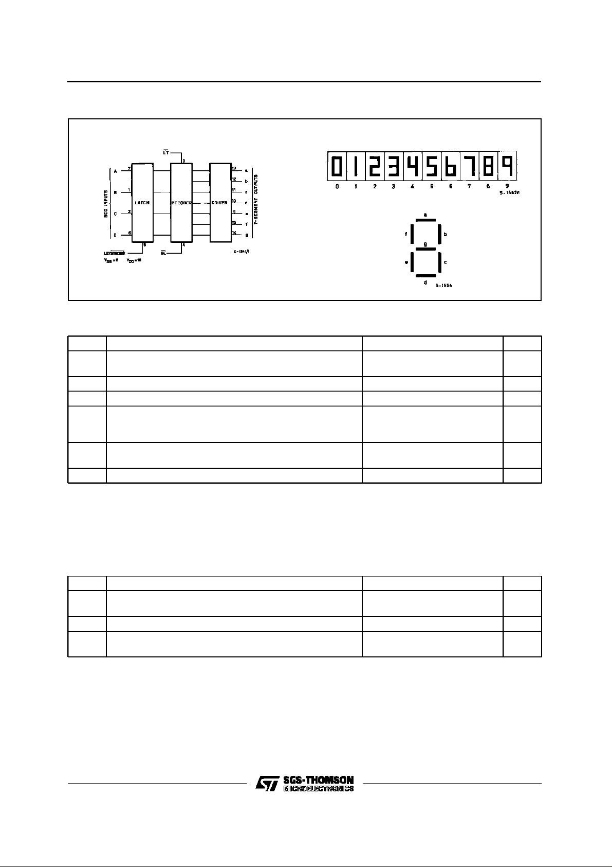
BCD-TO-SEVEN SEGMENT LATCH/DECODER/DRIVER
. HIGH-OUTPUT-SOURCING CAPABILITY (up
to 25 mA)
.INPUTLATCHES FOR BCD CODE STORAGE
.LAMP TEST AND BLANKING CAPABILITY
.7-SEGMENT OUTPUTS BLANKED FOR BCD
INPUTCODES > 1001
.QUIESCENT CURRENT SPECIFIED TO 20V
FOR HCC DEVICE
.STANDARDIZED SYMMETRICAL OUTPUT
CHARACTERISTICS
.5V, 10V, AND 15VPARAMETRIC RATINGS
.INPUTCURRENTOF100mAAT18V AND25°C
FOR HCC DEVICE
.100% TESTEDFOR QUIESCENTCURRENT
.MEETSALLREQUIREMENTSOFJEDECTEN-
TATIVESTANDARDN°13A,”STANDARDSPECIFICATIONS FOR DESCRIPTION OF ”B”
SERIESCMOS DEVICES”
HCC/HCF4511B
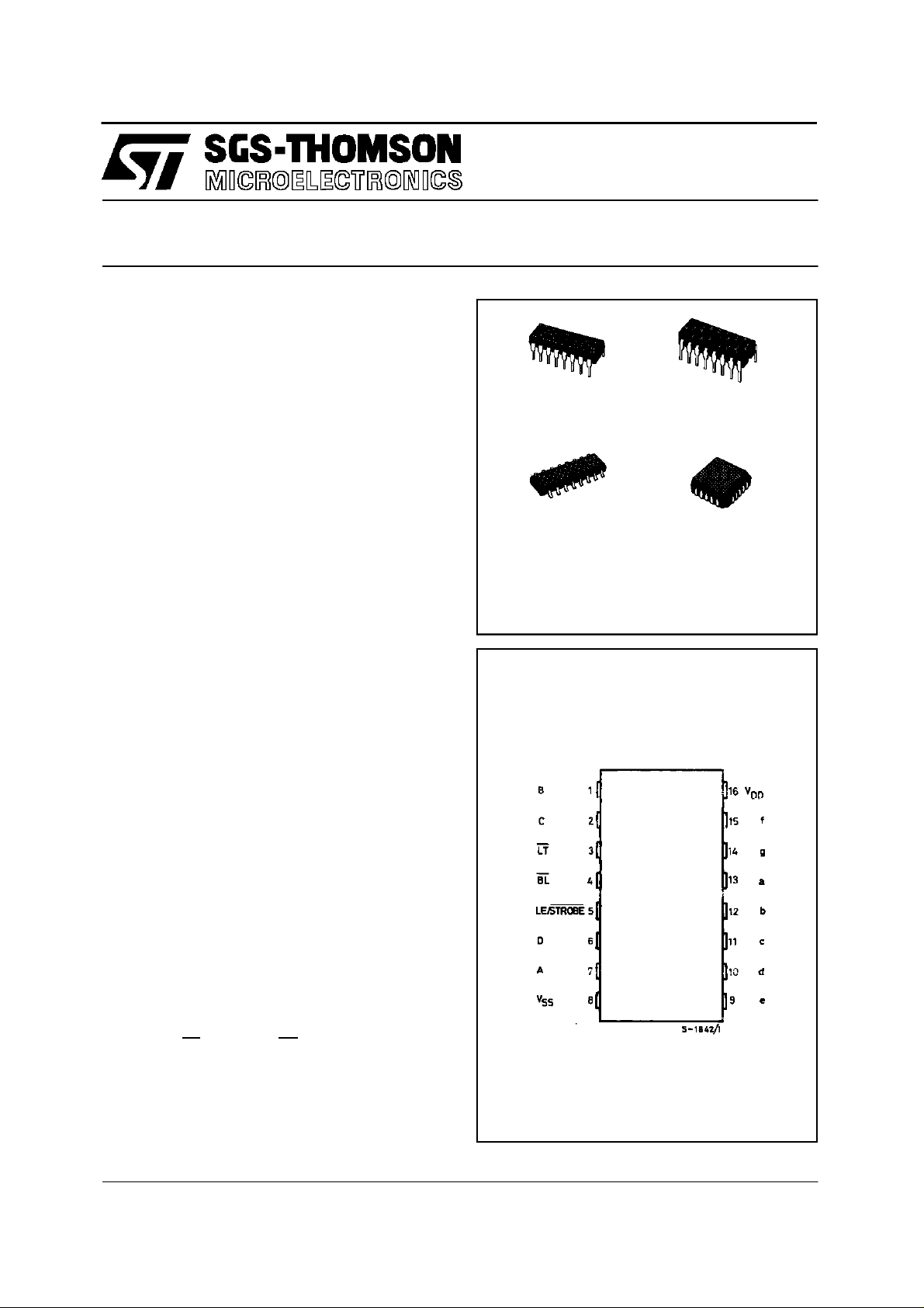
EY
(Plastic Package)
M1
(MicroPackage)
ORDERCODES :
HCC 4511BF HCF4511BM1
HCF4511BEY HCF4511BC1
(CeramicFrit Seal Package)
C1
(Plastic Chip Carrier)
F
DESCRI PTIO N
TheHCC4511B (extendedtemperature range) and
the HCF 4511B (intermediate temperature range)
are monolithic integrated circuits available in 16-lead dual in-line plastic or ceramic package and plastic micro package.
TheHCC/HCF4511B typesareBCD-to-7-segment
latch decoder drivers constructed with COS/MOS
logic and n-p-n bipolar transistor output deviceson
a singlemonolithic structure. These devices combine thelow quiescent powerdissipationandhighnoise immunity features of COS/MOS with n-p-n
bipolar output transistors capable of sourcingup to
25 mA. This capability allowsthe HCC/HCF4511B
typesto drive LED’s and other displays directly.
LampTest(LT), Blanking (BL), and LatchEnableor
Strobe inputs are provided to test the display, shut
off or intensity-modulate it, and store or strobe a
BCD code, respectively. Several different signal
may be multiplexed and displayed when external
multiplexing circuitry is used.
PIN CONNECTI O NS
November1996
1/16
Page 2
HCC/HFC4511B
FUN CTIONAL DIAG R A M
ABSOLUTE MAXIMUM RATIN GS
Symbol Parameter Value Unit
* Supply Voltage :HCC Types
V
DD
HCF Types
V
Input Voltage – 0.5 to VDD+ 0.5 V
i
DC Input Current (any one input) ± 10 mA
I
I
P
Total Power Dissipation (per package)
tot
Dissipation per Output Transistor
for T
T
Operating Temperature : HCC Types
op
= Full Package-temperature Range
op
HCF Types
T
Stresses abovethose listed under ”Absolute MaximumRatings”may cause permanent damage to the device. This is a stressrating only and
functionnal operation of the device at theseor any other conditions abovethose indicatedin theoperationalsections ofthis specification is not
implied.Exposure toabsolute maximum ratingconditions for external periods may affectdevice reliability.
*
Allvoltage values are referred to VSSpinvoltage.
Storage Temperature – 65 to + 150 °C
stg
– 0.5 to + 20
– 0.5 to + 18
200
100
– 55 to + 125
–40to+85
V
V
mW
mW
°C
°C
RECOMMENDED OPERATING CONDITIONS
Symbol Parameter Value Unit
V
T
2/16
Supply Voltage : HCC Types
DD
HCF Types
V
Input Voltage 0 to V
I
Operating Temperature : HCC Types
op
HCF Types
3to18
3to15
DD
– 55 to + 125
–40to+85
V
V
V
°C
°C
Page 3
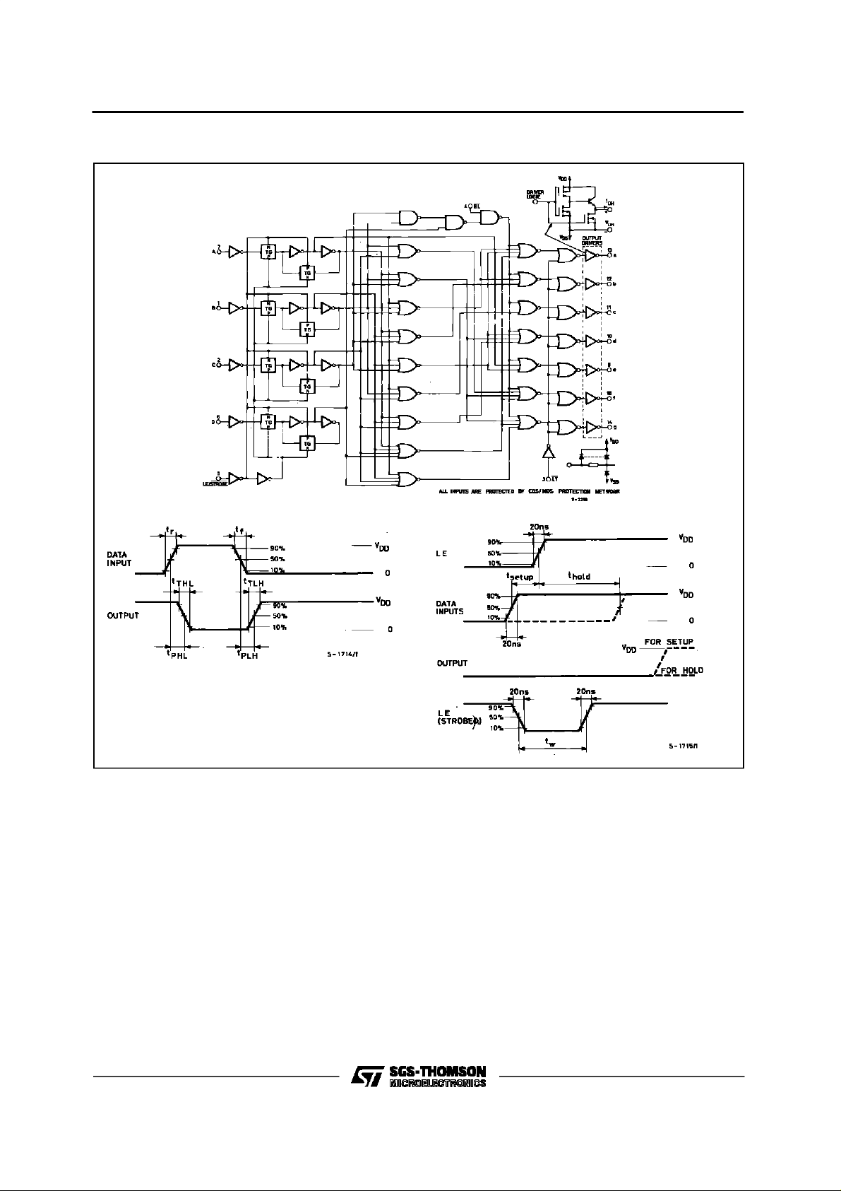
LOGIC DIAGRAMS
HCC/HCF4511B
3/16
Page 4
HCC/HFC4511B
TRUTH TABLE
LE BI LT D C B A a b c d e f g Display
XX0X X
X 0 1 X X X X 0 0 0 0 0 0 0 Blank
0110 0
0110 0
0110 0
0110 0
0110 1
0110 1
01101
0110 1
0111 0
0111 0
0 1 1 1 0 1 0 0 0 0 0 0 0 0 Blank
0 1 1 1 0 1 1 0 0 0 0 0 0 0 Blank
0 1 1 1 1 0 0 0 0 0 0 0 0 0 Blank
0 1 1 1 1 0 1 0 0 0 0 0 0 0 Blank
0 1 1 1 1 1 0 0 0 0 0 0 0 0 Blank
0 1 1 1 1 1 1 0 0 0 0 0 0 0 Blank
1 1 1 X X X X * *
X X 1 1 1 1 1 1 1
0 0 1 1 1 1 1 1 0
0 1 0 1 1 0 0 0 0
1 0 1 1 0 1 1 0 1
1 1 1 1 1 1 0 0 1
0 0 0 1 1 0 0 1 1
0 1 1 0 1 1 0 1 1
1 0 0 0 1 1 1 1 1
1 1 1 1 1 0 0 0 0
0 0 1 1 1 1 1 1 1
0 1 1 1 1 0 0 1 1
8
0
1
2
3
4
5
6
7
8
9
4/16
Page 5
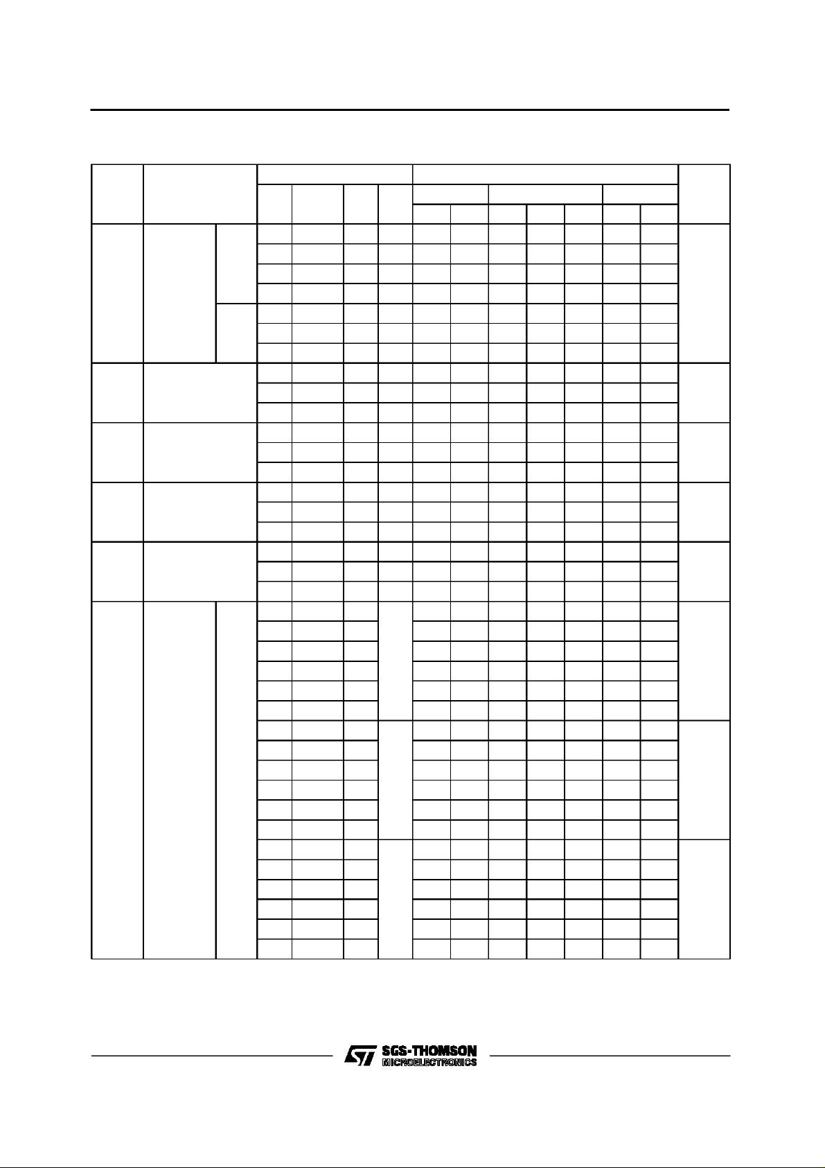
HCC/HCF4511B
STATIC ELECTRICAL CHARACTERISTICS (over recommended operating conditions)
Test Conditions Valu e
Symbol Parameter
I
Quiescent
L
Current
HCC
Types
HCF
Types
V
OH
Output High
Voltage
V
OL
Output Low
Voltage
V
IH
Input High
Voltage
V
IL
Input Low
Voltage
V
OH
Output
Drive
HCC
Types
Voltage
*T
=–55°C for HCC device : – 40°CforHCF device.
Low
*T
= +125°C for HCC device: + 85°C for HCF device.
High
TheNoise Marginfor both ”1” and”0” level is : 1V min. with VDD= 5V,2V min. withVDD=10V, 2.5 V min. withVDD= 15V.
V
V
O
|IO|V
I
(V) (V) (µA) (V)
T
DD
* 25°CT
Low
Min. Max. Min. Ty p. Max. Min. Max .
High
0/ 5 5 5 0.04 5 150
0/10 10 10 0.04 10 300
0/15 15 20 0.04 20 600
0/20 20 100 0.08 100 3000
0/ 5 5 20 0.04 20 150
0/10 10 40 0.04 40 300
0/15 15 80 0.04 80 600
0/ 5 5 4 4.1 4.55 4.2
0/10 10 9 9.1 9.55 9.2
0/15 15 14 14.1 14.55 14.2
5/0 5 0.05 0.05 0.05
10/0 10 0.05 0.05 0.05
15/0 15 0.05 0.05 0.05
0.5/3.8 5 3.5 3.5 3.5
1/8.8 10 7 7 7
1.5/13.8 15 11 11 11
3.8/0.5 5 1.5 1.5 1.5
8.8/1 10 3 3 3
13.8/1.5 15 4 4 4
0
4.1 4.10 4.55 4.20
5 4.25
10 3.80 3.90 4.10 3.90
5
15 3.95
20 3.55 3.40 3.75
25 3.40 3.10 3.55
0
9 9.10 9.55 9.20
5 9.25
10 8.85 9 9.15
10
15 9.05
20 8.70 8.60 8.90 8.40
25 8.60 8.30 8.75
0
14 14.10 14.55 14.20
5 14.30
10 13.90 14 14.20 14
15
15 14.10
20 13.75 13.70 13.95 13.50
25 13.65 13.50 13.80 13.10
Unit
*
µA
V
V
V
V
V
V
V
5/16
Page 6

HCC/HFC4511B
STATIC ELECTRICAL CHARACTERISTICS (continued)
Test Conditions Valu e
Symbol Parameter
V
OH
Output
Drive
Voltage
HCF
Types
I
OL
Output
Sink
Current
HCC
Types
HCF
Types
I
IH,IIL
Input
Leakage
Current
HCC
Types
HCF
Types
C
Input Capacitance Any Input 5 7.5 pF
I
*T
=–55°C for HCC device : – 40°CforHCF device.
Low
*T
= +125°C for HCC device: + 85°C for HCF device.
High
TheNoise Marginfor both ”1” and”0” level is : 1V min. with VDD= 5V,2V min. withVDD=10V, 2.5 V min. withVDD= 15V.
V
V
O
|IO|V
I
(V) (V) (µA) (V)
0
T
DD
* 25°CT
Low
Min. Max. Min. Ty p. Max. Min. Max .
4.1 4.1 4.57 4.1
5 4.24
10 3.6 3.6 4.12 3.3
5
15 3.94
20 2.8 2.8 3.75 2.5
25 3.54
0
9.1 9.1 9.58 9.1
5 9.26
10 8.75 8.75 9.17 8.45
10
15 9.04
20 8.1 8.1 8.90 7.8
25 8.75
0
14.1 14.1 14.59 14.1
5 14.27
10 13.75 13.75 14.18 13.45
15
15 14.07
20 13.1 13.1 13.95 12.8
25 13.80
0/ 5 0.4 5 0.64 0.51 1 0.36
0/10 0.5 10 1.6 1.3 2.6 0.9
0/15 1.5 15 4.2 3.4 6.8 2.4
0/ 5 0.4 5 0.52 0.44 1 0.36
0/10 0.5 10 1.3 1.1 2.6 0.9
0/15 1.5 15 3.6 3 6.8 2.4
0/18
18 ± 0.1 ±10
–5
± 0.1 ±1
Any Input
0/15
15 ±0.3 ±10
–5
± 0.3 ± 1
High
Unit
*
V
V
V
mA
µA
6/16
Page 7

HCC/HCF4511B
DYNAMIC ELECTRICAL CHARACTERISTICS (T
=25oC, CL=50pF,RL= 200 KΩ,
amb
typic al temperature coeffic ent for all VDDvalues is 03 %/oC, all input rise and fall tim es = 20 ns)
Symbol Parameter
t
PHL
t
PLH
t
PHL
t
PLH
t
PHL
t
PLH
t
t
t
setup
t
Propagation Delay Time (data) 5 520 1040
Propagation Delay Time (data) 5 660 1320
Propagation Delay Time (BL) 5 350 700
Propagation Delay Time (BL) 5 400 800
Propagation Delay Time (LT) 5 250 500
Propagation Delay Time (LT) 5 150 300
Transition Time 5 40 80
TLH
Transition Time 5 125 310
THL
Setup Time 5 150 75
Hold Time 5 0 -75
hold
Strobe Pulse Width 5 400 200
t
W
Test Conditions Value
(V) Min. Typ. Max.
V
DD
10 210 420
15 150 300
10 260 520
15 180 360
10 175 350
15 125 250
10 175 350
15 150 300
10 125 250
15 85 170
10 75 150
15 50 100
10 30 60
15 20 40
10 75 185
15 65 160
10 70 35
15 40 20
10 0 -35
15 0 -20
10 160 80
15 100 50
Unit
ns
ns
ns
ns
ns
ns
ns
ns
ns
ns
ms
7/16
Page 8

HCC/HFC4511B
TypicalOutputLow (sink) Current Characteristics. Typical data-to-output, low-to-high-level propaga-
tion delay time as a function of load capacitance.
Typicaldata-to-output, high-to-low-level propagation delay time as a function of loadcapacitance.
Typical high-to-low level transition ime as a function of load capacitance.
Typicallow-to-high level transitionime as a function of load capacitance.
TypicalVoltage drop (VDDtooutput) vs. Output
source Current as a Function of Supply.
8/16
Page 9

HCC/HCF4511B
TypicalDynamic Power Dissipation Charac-
Derated Static Output Current PerOutput.
teristics.
Maximumcontinuous derated output currentIOH appliesto a single
outputwith allother outputs sourcing an equalamount of currentat
the supplyvoltages shown. Operationabove the deratingcurve is
not recommenced.
TYPICAL APPLICA TI ONS (inter faci ng w ith variou s disp lays)
DRIVINGCOMMON-CATHODE 7-SEGMENT LED DISPLAYS
9/16
Page 10

HCC/HFC4511B
TYPICAL APPLICA TI ONS (cont inued)
Driving Low-voltage Fluorescent Displays. Driving Incandescent Displays.
Amedium-brightness intensitydisplay can be obtained withlowvoltagefluorescent displays such as the Tung-Sot Digivac S/G
series.
TEST CIRCUITS
QuiescentDevice Current.
Input Leakage Current.
2 of 7 SegmentsShownConnected
Resistors R from VDD VDD to each 7-segment driver output
arechoosen to keep allNumitronsegments slightlyon and
warm.
Noise Immunity.
Data Propagation Delay.
10/16
Page 11

TEST CIRCUITS (contin ue d)
Dynamic Power dissipation.
HCC/HCF4511B
11/16
Page 12

HCC/HFC4511B
Plastic DIP16 (0.25) MECHANICAL DATA
DIM.
MIN. TYP. MAX. MIN. TYP. MAX.
a1 0.51 0.020
B 0.77 1.65 0.030 0.065
b 0.5 0.020
b1 0.25 0.010
D 20 0.787
E 8.5 0.335
e 2.54 0.100
e3 17.78 0.700
F 7.1 0.280
I 5.1 0.201
L 3.3 0.130
Z 1.27 0.050
mm inch
12/16
P001C
Page 13

Ceramic DIP16/1 MECHANICAL DATA
HCC/HCF4511B
DIM.
MIN. TYP. MAX. MIN. TYP. MAX.
A 20 0.787
B 7 0.276
D 3.3 0.130
E 0.38 0.015
e3 17.78 0.700
F 2.29 2.79 0.090 0.110
G 0.4 0.55 0.016 0.022
H 1.17 1.52 0.046 0.060
L 0.22 0.31 0.009 0.012
M 0.51 1.27 0.020 0.050
N 10.3 0.406
P 7.8 8.05 0.307 0.317
Q 5.08 0.200
mm inch
P053D
13/16
Page 14

HCC/HFC4511B
SO16 (Narrow) MECHANICAL DATA
DIM.
MIN. TYP. MAX. MIN. TYP. MAX.
A 1.75 0.068
a1 0.1 0.2 0.004 0.007
a2 1.65 0.064
b 0.35 0.46 0.013 0.018
b1 0.19 0.25 0.007 0.010
C 0.5 0.019
c1 45° (typ.)
D 9.8 10 0.385 0.393
E 5.8 6.2 0.228 0.244
e 1.27 0.050
e3 8.89 0.350
F 3.8 4.0 0.149 0.157
G 4.6 5.3 0.181 0.208
L 0.5 1.27 0.019 0.050
M 0.62 0.024
S8°(max.)
mm inch
14/16
P013H
Page 15

PLCC20 MECHANICAL DATA
HCC/HCF4511B
DIM.
MIN. TYP. MAX. MIN. TYP. MAX.
A 9.78 10.03 0.385 0.395
B 8.89 9.04 0.350 0.356
D 4.2 4.57 0.165 0.180
d1 2.54 0.100
d2 0.56 0.022
E 7.37 8.38 0.290 0.330
e 1.27 0.050
e3 5.08 0.200
F 0.38 0.015
G 0.101 0.004
M 1.27 0.050
M1 1.14 0.045
mm inch
P027A
15/16
Page 16

HCC/HFC4511B
Information furnished is believed to be accurate and reliable. However, SGS-THOMSONMicroelectronics assumes no responsability for the
consequences of use of such informationnor for any infringement of patents or other rights of third partieswhich may results from its use. No
licenseis grantedby implication or otherwise under any patent or patent rights of SGS-THOMSONMicroelectronics. Specifications mentioned
in this publication are subject to changewithoutnotice. Thispublication supersedes andreplacesall information previously supplied.
SGS-THOMSONMicroelectronics products are notauthorizedfor use ascriticalcomponents in lifesupport devices or systems without express
writtenapproval ofSGS-THOMSONMicroelectonics.
1996 SGS-THOMSONMicroelectronics -Printedin Italy- AllRightsReserved
Australia- Brazil -Canada - China - France- Germany- Hong Kong - Italy - Japan- Korea- Malaysia - Malta - Morocco- The Netherlands -
Singapore - Spain - Sweden- Switzerland-Taiwan - Thailand- UnitedKingdom - U.S.A
SGS-THOMSONMicroelectronics GROUPOF COMPANIES
.
16/16
 Loading...