

■ 1 TTL-LOADOUTPUTDRIVE CAPABILITY
■ 2 OUTPUT-DISABLECONTROLS
■ 3STATEOUTPUTS
■ 5V,10V,AND15VPARAMETRICRATINGS
■ QUIESCENTCU R R ENTSPEC IFIEDUPTO
15V
■ INPUT CURRENT OF300nA AT 15VAND
25°C
■ 100%TEST EDFOR QUIESCENTCU R R EN T
MEETS ALL REQUIREMENTS OF JEDEC
TENTATIVE STANDARD N
0
. 13A, ”STANDARD
SPECIFICATIONS FOR DESCRIPTION OF ”B”
SERIESCMOS DEVICES”
DESCRIPTION
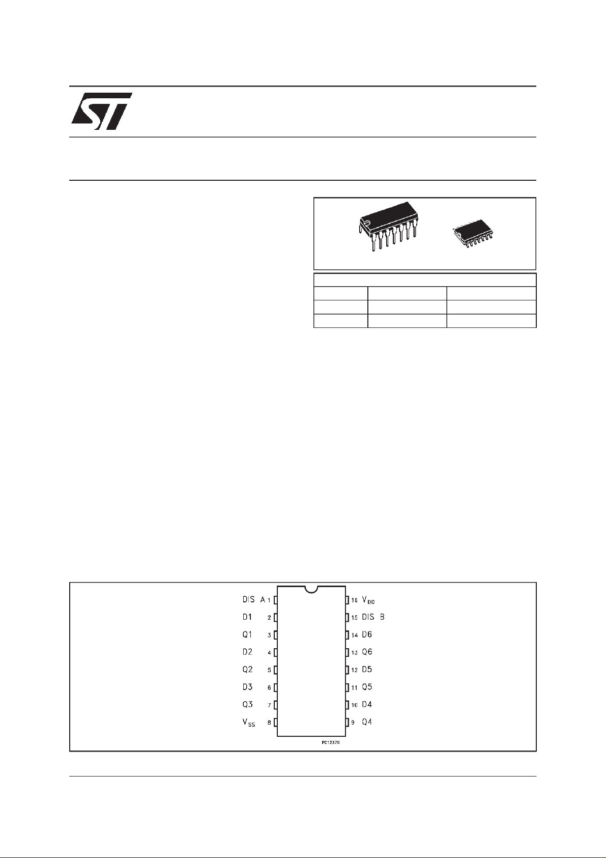
The HCF4503B is a monolithicintegrated circuits,
available in 16-lead dual in-line plastic package
and plastic micro package.
HCF4503
HEX BUFFER
SOPDIP
ORDER CODES
PACK AG E TUBE T & R
DIP HCF4503BEY
SOP HCF4503BM1 HCF4503M013TR
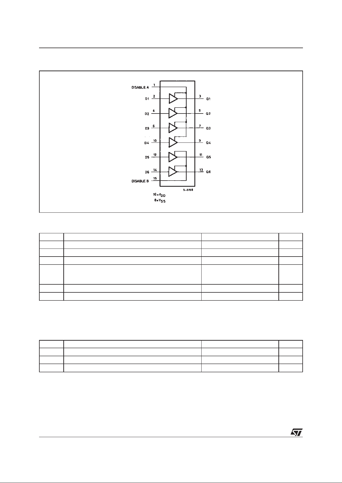
The HCF4503B is a hex noninverting buffer with
3-state outputs having high sink and
source-current capability. Two disable controls
are provided, one of which controls four buffers
and the other controls the remainingtwo buffers.
PIN CONNECTION
February 2000
1/10
HCF4503B
FUNCTIONAL DIAGRAM
ABSOLUTE MAXIMUM RATING
Symb o l Parameter Val u e Uni t
* Supply Voltage -0.5 to +18 V
V
DD
Input Voltage -0.5 to VDD+ 0.5 V
V
i
DC Input Current (any one input) ± 10 mA
I
I
Total Power Dissipation (per package)
P
tot
200
mW
Dissipation per Output Transistor
for Top = Full Package Temperature Range
T
Operating Temperature -40 to +85
op
Storage Temperature -65 to +150
T
stg
Stresses above those listedunder ”Absolute Maximum Ratings” may cause permanent damage to thedevice. Thisisa stress rating only and functional
operation ofthedevice atthese orany otherconditions above those indicated inthe ope rational sections of this specification is not implied. Exposure to
abso lute max im u mratingconditio n s for externalperiod smayaffect devicereliability.
*Allvoltagevalues arereferredtoV
pinvoltage.
SS
100
mW
o
C
o
C
RECOMMENDED OPERATING CONDITIONS
Symb o l Parameter Val u e Uni t
V
Supply Voltage 3 to 15 V
DD
Input Voltage 0 to V
V
I
Operating Temperature -40 to +85
T
op
DD
V
o
C
2/10
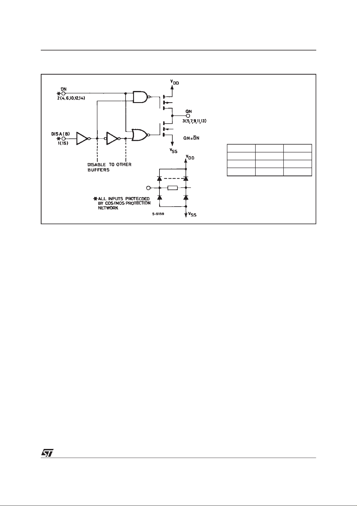
LOGICDIAGRAM AND TRUTH TABLE
HCF4503B
DN DIS A (B) QN
000
101
X 1 High Z
X= Don’tcare
3/10

HCF4503B
STATICELECTRICAL CHARACTERISTICS
(over recommendedoperatingconditions)
Symb o l Parameter Test C o n ditios Value Uni t
V
|I
|
V
I
(V)
Quiescent Current 0/5 5 4 0.02 4 30
I
L
O
(V)
O
(µA)
V
(V)
DD
o
-40
C25
Mi n . Max. Mi n . Typ. M ax. Min. Max.
0/10 10 8 0.02 8 60
o
C85
o
C
µ
0/15 15 16 0.02 16 120
V
OH
Output High
Voltage
0/5 < 1 5 4.95 4.95 4.95
0/10 < 1 10 9.95 9.95 9.95
0/15 < 1 15 14.95 14.95 14.95
V
OL
Output Low
Voltage
5/0 < 1 5 0.05 0.05 0.05
10/0 < 1 10 0.05 0.05 0.05
15/0 < 1 15 0.05 0.05 0.05
V
IH
Input High
Voltage
0.5/4.5 < 1 5 3.5 3.5 3.5
1/9 < 1 10 7 7 7
1.5/13.5 < 1 15 11 11 11
V
IL
Input Low
Voltage
4.5/0.5 < 1 5 1.5 1.5 1.5
9/1 < 1 10 3 3 3
13.5/1.5 < 1 15 4 4 4
I
OH
Output Drive
Current
0/5 2.5 5 -4.8 -4.1 -5.2 -2.9
0/5 4.6 5 -1 -0.8 -1.6 -0.6
mA
0/10 9.5 10 -2.5 -2.2 -3.1 -1.6
0/15 13.5 15 -6.8 -5.8 -11.9 -4.2
Output Sink Current 0/5 0.4 5 2.1 1.8 1.9 1.2
I
OL
0/10 0.5 10 5.4 4.7 5.3 3.3
mA
0/15 1.5 15 16 13.7 19.5 9.7
I
IH,IIL
Input Leakage
Current
3-state Output
I
OZ
Leakage Current
Input Capacitance Any Input 5 7.5
C
I
TheNoiseMargin forboth”1”and”0”levelis:1Vmin.withVDD=5V,2Vmin.withVDD=10V,2.5Vmin.withVDD=15V
0/15 Any
Input
0/15 Any
Input
15
15
±
±
0.3
1.0
-5
0.3
10
±
±
-4
1.0
10
±
±
±
±
7.5
1
µ
µ
pF
A
V
V
V
V
A
A
4/10

HCF4503B
DYNAMICELECTRICAL CHARACTERISTICS
typicaltemperaturecoefficentforallV
valuesis 03%/oC, allinput rise andfalltimes= 20 ns)
DD
=25oC, CL=50pF,RL= 200KΩ,
(T
amb
Symb o l Parameter Test C o n ditions Valu e Uni t
V
Min. Typ. Max.
DD
(V)
t
Propagation Delay Time 5 75 150
PLH
10 35 70
ns
15 25 50
t
Propagation Delay Time 5 55 110
PHL
10 25 50
ns
15 17 35
t
3-State Propagation Delay Time 5 70 140
PHZ
t
PZH
10 30 60
ns
15 25 50
t
3-State Propagation Delay Time 5 90 180
t
PZL
PLZ
10 40 80
ns
15 35 70
t
Transition Time 5 50 90
TLH
10 30 45
ns
15 25 35
t
Transition Time 5 35 70
THL
10 20 40
ns
15 13 25
N-Channel OutputLow(sink)Current
Characteristics.
P-Channel OutputHigh (source) Current
Characteristics.
5/10

HCF4503B
TypicalPropagationDelayTime vs.Load
Capacitance.
TypicalDynamic Power Dissipationvs.
TypicalTransition Time vs. Load Capacitance.
TESTCIRCUITS
QuiescentDevice Current.
6/10
InputVoltage.

HCF4503B
TESTCIRCUIT
(continued)
InputLeakageCurrent. DynamicPower Dissipation.
7/10

HCF4503B
Plastic DIP-14 MECHANICALDATA
DIM.
MIN. TYP. MAX. MIN. TYP. MAX.
a1 0.51 0.020
B 1.39 1.65 0.055 0.065
b 0.5 0.020
b1 0.25 0.010
D 20 0.787
E 8.5 0.335
e 2.54 0.100
e3 15.24 0.600
F 7.1 0.280
I 5.1 0.201
L 3.3 0.130
Z 1.27 2.54 0.050 0.100
mm inch
8/10
P001A

SO-14 MECHANICAL DATA
HCF4503B
DIM.
MIN. TYP. MAX. MIN. TYP. MAX.
A 1.75 0.068
a1 0.1 0.2 0.003 0.007
a2 1.65 0.064
b 0.35 0.46 0.013 0.018
b1 0.19 0.25 0.007 0.010
C 0.5 0.019
c1 45 (typ.)
D 8.55 8.75 0.336 0.344
E 5.8 6.2 0.228 0.244
e 1.27 0.050
e3 7.62 0.300
F 3.8 4.0 0.149 0.157
G 4.6 5.3 0.181 0.208
L 0.5 1.27 0.019 0.050
M 0.68 0.026
S 8 (max.)
mm inch
P013G
9/10

HCF4503B
Information furnished isbelieved tobeaccurate and reliable.However, STMicroelectronicsassumes no responsibility for the consequences
of use of such information nor for any infringement of patents or other rights of third parties which may result from its use. No license is
granted by implicationor otherwise under any patent or patent rights of STMicroelectronics. Specification mentioned in thispublication are
subject tochange without notice. Thispublication supersedes and replaces all information previously supplied. STMicroelectronics products
are not authorized for use as critical components in life support devices or systems withoutexpress written approval of STMicroelectronics.
The ST logo is a registeredtrademark of STMicroelectronics
2000 STMicroelectronics – Printed in Italy – All Rights Reserved
STMicroelectronics GROUP OF COMPANIES
Australia - Brazil- China- Finland - France -Germany - Hong Kong - India - Italy - Japan- Malaysia - Malta - Morocco
Singapore - Spain- Sweden- Switzerland - United Kingdom - U.S.A.
http://www.st.com
.
10/10
 Loading...