

Page 1

STROBED HEX INVERTER/BUFFER
. 2 TTL-LOAD OUTPUTDRIVECAPABILITY
.3-STATE OUTPUTS
.COMMONOUTPUT-DISABLE CONTROL
.INHIBITCONTROL
.QUIESCENT CURRENT SPECIFIED TO 20V
FOR HCC DEVICE
.5V, 10V,AND 15VPARAMETRIC RATINGS
.INPUTCURRENTOF100nAAT18V AND25°C
FOR HCC DEVICE
.100%TESTEDFOR QUIESCENTCURRENT
.MEETSALLREQUIREMENTSOFJEDECTEN-
TATIVE STANDARD N°. 13A, ”STANDARD
SPECIFICATIONS FOR DESCRIPTIONOF”B”
SERIESCMOSDEVICES”
HCC/HCF4502B
EY
(Plastic Package)
M1
MicroPackage
ORDERCODES :
HCC4502BF HCF4502BM1
HCF4502BEY HCF4502BC1
(Ceramic Frit SealPackage)
F
C1
(Plastic ChipCarrier)
DESCRI PTIO N
TheHCC4502B(extended temperature range) and
HCF4502B (intermediate temperature range) are
monolithic integrated circuit, available in 16-lead
dual in-line plastic or ceramic package and plastic
micro package. The HCC/HCF 4502B consists of
six inverter-buffers with 3-state outputs. A logic ”1”
on the OUTPUT DISABLE input produces a highimpedance state in all sixoutputs. This feature permitscommonbusing ofthe outputs, thussimplifying
systemdesign. A logic”1” ontheINHIBITinputswitches all six outputs to logic”0” iftheOUTPUTDISABLE input is a logic ”0”. This device is capable of
driving two standard TTLloads, whichisequivalent
to six times the JEDEC ”B” series IOLstandard.
PIN CO N NEC TI O NS
June 1989
1/11
Page 2

HCC/HCF4502B
ABSOLUTE M AXI MUM RATIN G S
Symbol Parameter Value Unit
V
* Supply Voltage :HC C Types
DD
HCF Types
V
Input Voltage – 0.5 to VDD+ 0.5 V
i
I
DC Input Current (any one input) ± 10 mA
I
P
Total Power Dissipation (per package)
tot
Dissipation per Output Transistor
for Top= Full Package-temperature Range
T
Operating Temperature : HCC Types
op
HCF Types
T
Stresses above those listed under ”Absolute Maximum Ratings” may cause permanent damage to the device. This is a stress
rating only and functional operation of the device at these or any other conditions above those indicated in the operational sections of this specification is not implied. Exposure to absolute maximum rating conditions for external periods may affect device
reliability.
*
Allvoltage values arereferredto VSSpinvoltage.
Storage Temperature – 65 to + 150 °C
stg
RECOMMENDED OPERATING CONDITIONS
Symbol Parameter Value Unit
V
T
Supply Voltage : HC C Types
DD
HCF Types
V
Input Voltage 0 to V
I
Operating Temperature : HCC Types
op
HCF Types
– 0.5 to + 20
– 0.5 to + 18
200
100
– 55 to + 125
–40to+85
3to+18
3to+15
DD
– 55 to + 125
–40to+85
V
V
mW
mW
°C
°C
V
V
V
°C
°C
TRUTH TABLE
Disab le Inh ib i t D n Qn
0001
00I0
0IX0
IXXZ
X = don’t care
Z = high impedance
Logic 1 = high
Logic 0 = low
2/11
Page 3

HCC/HCF4502B
STATIC ELECTRICAL CHARACTERISTICS (over recommended operating conditions)
Test Conditions Value
V
V
Symbol Parameter
I
Quiescent
L
Current
HCC
Types
I
(V) (V) (µA) (V)
0/ 5 5 1 0.02 1 30
0/10 10 2 0.02 2 60
0/15 15 4 0.02 4 120
O
|IO|V
DD
0/20 20 20 0.04 20 600
0/ 5 5 4 0.02 4 30
HCF
Types
OH
Output High
V
Voltage
0/10 10 8 0.02 8 60
0/15 15 16 0.02 16 120
0/ 5 < 1 5 4.95 4.95 4.95
0/10 < 1 10 9.95 9.95 9.95
0/15 < 1 15 14.95 14.95 14.95
OL
Output Low
V
Voltage
5/0 < 1 5 0.05 0.05 0.05
10/0 < 1 10 0.05 0.05 0.05
15/0 < 1 15 0.05 0.05 0.05
V
IH
Input High
Voltage
0.5/4.5 < 1 5 3.5 3.5 3.5
1/9 < 1 10 7 7 7
1.5/13.5 < 1 15 11 11 11
IL
Input Low
V
Voltage
4.5/0.5 < 1 5 1.5 1.5 1.5
9/1 < 1 10 3 3 3
13.5/1.5 < 1 15 4 4 4
I
OH
Output
Drive
Current
HCC
Types
0/ 5 2.5 5 – 2 – 1.6 – 3.2 –1.15
0/ 5 4.6 5 –0.64 –0.51 – 1 –0.36
0/10 9.5 10 – 1.6 – 1.3 – 2.6 – 0.9
0/15 13.5 15 – 4.2 – 3.4 – 6.8 – 2.4
0/ 5 2.5 5 –1.53 –1.36 – 3.2 – 1.1
HCF
Types
0/ 5 4.6 5 –0.52 –0.44 – 1 –0.36
0/10 9.5 10 – 1.3 – 1.1 – 2.6 – 0.9
0/15 13.5 15 – 3.6 – 3.0 – 6.8 – 2.4
OL
Output
Sink
Current
HCC
Types
I
0/ 5 0.4 5 3.84 3.06 6 2.10
0/10 0.5 10 9.6 7.8 15.6 5.4
0/15 1.5 15 25.2 20.4 40.8 14.4
0/ 5 0.4 5 3.11 2.6 6 2.10
HCF
Types
I
IH,IIL
Input
Leakage
Current
HCC
Types
HCF
Types
I
OH,IOL
3-state
Output
HCC
Types
HCF
Types
C
Input Capacitance Any Input 5 7.5 pF
I
*T
=–55°CforHCC device : – 40°CforHCF device.
Low
*T
=+125°C for HCC device : + 85°C for HCF device.
High
TheNoise Margin for both”1” and”0” levelis : 1Vmin. with VDD=5V, 2V min. with VDD= 10V,2.5V min.with VDD= 15V.
0/10 0.5 10 7.05 6.63 15.6 5.61
0/15 1.5 15 20.4 17.3 40.8 14.2
0/18
18 ± 0.1 ±10
Any Input
0/15
15 ± 0.3 ±10
0/18 18 ± 0.4 ±10
0/15 15 ± 1.0
T
* 25°CT
Low
Min. Max. Min. Typ. Max. Min. Max.
–5
± 0.1 ± 1
–5
± 0.3 ± 1
–4
± 0.4 ± 12
–4
± 1.0 ± 7. 5
±10
High
*
Unit
µA
V
V
V
V
mA
mA
µA
µA
3/11
Page 4

HCC/HCF4502B
DYNAMIC ELECTRICAL CHARACTERISTICS (T
=25°C,CL= 50 pF, RL= 200 kΩ
amb
typical temperature coefficient for all VDDvalues is 0.3 %/°C, all input rise and fall times = 20 ns)
Symbol Parameter
t
PHL
t
PLH
t
PHZ
Data or Inhibit Delay Time 5 135 270
Data or Inhibit Delay Time 5 190 380
Disable Delay Time (output high
to high impedance)
t
PZH
Disable Delay Time (high
impedance to output high)
t
PL Z
Disable Delay Time (output low to
high impedance)
t
PZL
Disable Delay Time (high
impedance to output low)
t
t
TLH
THL
Tansition Time 5 100 200
Transition Time 5 60 120
Test Conditions Value
V
(V) Min. Typ. Max.
DD
10 60 120
15 40 80
10 90 180
15 65 30
560120
10 40 80
15 30 60
5110220
10 50 100
15 40 80
5125250
10 65 130
15 55 110
5125250
10 55 110
15 40 80
10 50 100
15 40 80
10 30 60
15 20 40
Unit
ns
ns
ns
ns
ns
ns
ns
ns
teristics.
4/11
TypicalOutput Low (sink) Current.Minimum Output High (source) Current Charac-
Page 5

HCC/HCF4502B
Minimum Output Low (sink) Current Characteristics.
TypicalOutput High (source) Current Characteristics.
TypicalTransition Time vs. Load Capacitance. Typical Propagation Delay Time vs. Load Capacit-
ance.
TEST CIRCUIT
QuiescentDevice Current. Input Voltage.
5/11
Page 6

HCC/HCF4502B
TEST CIRCUIT (continued)
Input Leakage Current.
TEST CIRCUITAND WAVEFORMS
DisableDelayTime.
Test Conditions
Test Pin 1 5 Point A
t
t
t
t
PHZ
PZH
PLZ
PZL
V
SS
V
DD
V
DD
V
SS
6/11
V
SS
V
DD
V
DD
V
SS
Page 7

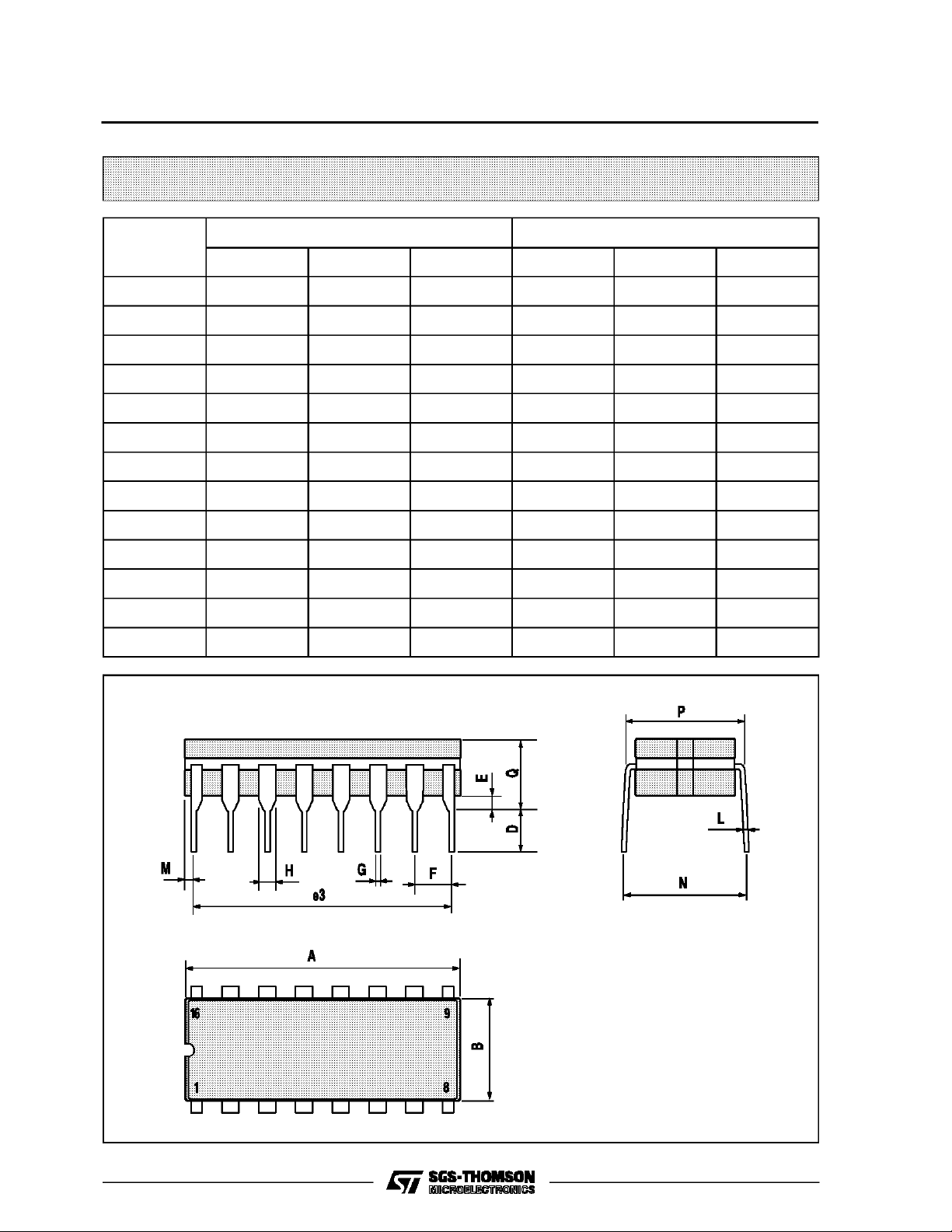
Plastic DIP16 (0.25) MECHANICAL DATA
HCC/HCF4502B
DIM.
MIN. TYP. MAX. MIN. TYP. MAX.
a1 0.51 0.020
B 0.77 1.65 0.030 0.065
b 0.5 0.020
b1 0.25 0.010
D 20 0.787
E 8.5 0.335
e 2.54 0.100
e3 17.78 0.700
F 7.1 0.280
I 5.1 0.201
L 3.3 0.130
Z 1.27 0.050
mm inch
P001C
7/11
Page 8
HCC/HCF4502B
Ceramic DIP16/1 MECHANICAL DATA
DIM.
MIN. TYP. MAX. MIN. TYP. MAX.
A 20 0.787
B 7 0.276
D 3.3 0.130
E 0.38 0.015
e3 17.78 0.700
F 2.29 2.79 0.090 0.110
G 0.4 0.55 0.016 0.022
H 1.17 1.52 0.046 0.060
L 0.22 0.31 0.009 0.012
M 0.51 1.27 0.020 0.050
N 10.3 0.406
P 7.8 8.05 0.307 0.317
Q 5.08 0.200
mm inch
8/11
P053D
Page 9

SO16 (Narrow) MECHANICAL DATA
HCC/HCF4502B
DIM.
MIN. TYP. MAX. MIN. TYP. MAX.
A 1.75 0.068
a1 0.1 0.2 0.004 0.007
a2 1.65 0.064
b 0.35 0.46 0.013 0.018
b1 0.19 0.25 0.007 0.010
C 0.5 0.019
c1 45° (typ.)
D 9.8 10 0.385 0.393
E 5.8 6.2 0.228 0.244
e 1.27 0.050
e3 8.89 0.350
F 3.8 4.0 0.149 0.157
G 4.6 5.3 0.181 0.208
L 0.5 1.27 0.019 0.050
M 0.62 0.024
S8°(max.)
mm inch
P013H
9/11
Page 10

HCC/HCF4502B
PLCC20 MECHANICAL DATA
DIM.
MIN. TYP. MAX. MIN. TYP. MAX.
A 9.78 10.03 0.385 0.395
B 8.89 9.04 0.350 0.356
D 4.2 4.57 0.165 0.180
d1 2.54 0.100
d2 0.56 0.022
E 7.37 8.38 0.290 0.330
e 1.27 0.050
e3 5.08 0.200
F 0.38 0.015
G 0.101 0.004
M 1.27 0.050
M1 1.14 0.045
mm inch
10/11
P027A
Page 11

HCC/HCF4502B
Information furnished is believed to be accurate and reliable. However, SGS-THOMSON Microelectronics assumesno responsability for the
consequences of use of such information norfor any infringement of patents or other rights of third partieswhich mayresults from its use.No
license isgrantedby implicationor otherwiseunderany patentor patentrights ofSGS-THOMSONMicroelectronics. Specificationsmentioned
in this publicationare subjectto change without notice. This publication supersedes andreplaces all informationpreviously supplied.
SGS-THOMSON Microelectronicsproductsare notauthorizedforuse ascritical componentsinlife supportdevicesorsystems withoutexpress
written approvalof SGS-THOMSONMicroelectonics.
1994 SGS-THOMSONMicroelectronics - All Rights Reserved
Australia - Brazil - France- Germany - HongKong - Italy - Japan - Korea- Malaysia -Malta - Morocco- The Netherlands -
Singapore -Spain - Sweden- Switzerland -Taiwan - Thailand- United Kingdom - U.S.A
SGS-THOMSON Microelectronics GROUP OF COMPANIES
11/11
 Loading...