

DUAL MONOSTABLE MULTIVIBRATOR
.RETRIGGERABLE/RESETTABLE CAPABILITY
.TRIGGER AND RESET PROPAGATION DE-
LAYS INDEPENDENTOF RX,C
X
.TRIGGERING FROM LEADING OR TRAILING
EDGE
.Q AND Q BUFFERED OUTPUTS AVAILABLE
.SEPARATERESETS
.WIDE RANGE OF OUTPUT-PULSE WIDTHS
.QUIESCENT CURRENT SPECIFIED TO 20V
FOR HCC DEVICE
.5V, 10V,AND 15VPARAMETRIC RATINGS
.INPUT CURRENT OF 100nA AT 18V AND
25°C FORHCC DEVICE
.100% TESTEDFOR QUIESCENTCURRENT
.MEETSALLREQUIREMENTSOFJEDECTEN-
TATIVE STANDARD N° 13A, ”STANDARD
SPECIFICATIONS FOR DESCRIPTIONOF ”B”
SERIESCMOS DEVICES”
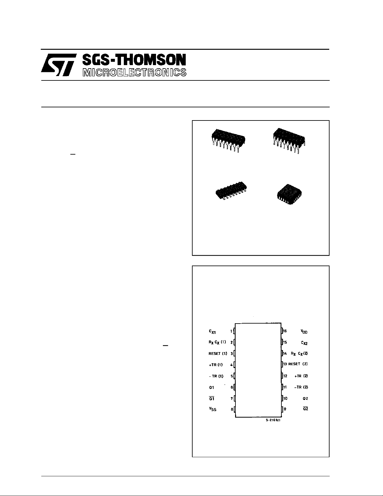
HCC/HCF4098B
EY
(Plastic Package)
M1
(MicroPackage)
ORDERCODES :
HCC4098BF HCF4098BM1
HCF4098BEY HCF4098BC1
(Ceramic Frit Seal Package)
F
C1
(PlasticChip Carrier)
DESCRIPTION
TheHCC4098B(extended temperature range) and
HCF4098B (intermediate temperature range) are
monolithic integrated circuit, available in 16-lead
dual in-line dual in-line plastic or ceramic package
and plastic micropackage. The HCC/HCF4098B
dualmonostablemultivibrator providesstableretriggerable/resettable one-shot operation for any fixedvoltage timing application. An external resistor (RX)
and anexternal capacitor(CX) controlthetiming for
the circuit.Adjustment of RXand CXprovides a wide
range of outputpulse widths from theQ and Q terminals. The time delay from trigger input to output
transition (trigger propagation delay) and the time
delayfromreset input tooutput transition (reset propagation delay) are independent of RXand CX.
Leading-edge-triggering (+ TR) and trailing-edgetriggering (– TR) inputs are provided for triggering
from either edge of an input pulse. An unused + TR
input should be tied to VSS. An unused – TR input
shouldbetiedto VDD. ARESET(on lowlevel)isprovidedfor immediate termination of the outputpulse
ortoprevent outputpulseswhenpoweristurnedon.
AnunusedRESETinputshouldbetiedtoVDD.However, if an entire section of the 4098B is not used,
its RESETshouldbetied to VSS. See table I. Innormal operation the circuit triggers (extends theoutput
PIN CONNECTIONS
June 1989
1/14

HCC/HCF4098B
pulse one period) on the application of each new
trigger pulse. For operation in the non-triggerable
mode, Q is connected to –TR when leading-edge
triggering (+ TR) is used or Q is connected to + TR
when trailing-edge triggering(–TR)isused.Thetime
period (T) for this multivibrator can be approximated
by TX=1/2 RXCXforCX≥ 0.01 µF.Timeperiods as
a function of RXforvalues of CXand VDDare given in
fig.8.ValuesofT varyfromunit tounitand asa functionofvoltage,temperature,andRXCX.Theminimum
value of external resistance, RX,is5kΩ. The maxi-
FUNCTIONAL DIAGRAM
mum value of external capacitance, CX, is 100µF.
Fig.9showstimeperiods asafunctionofCXforvalues
of RXand VDD. The output pulse width has variations of ± 2.5%typically, overthe temperature range
of– 55°Cto 125°CforCX=1000pF and RX=100
kΩ.Forpower supplyvariations of ± 5%,the output
pulsewidthhas variationsof ±0.5%typically, forV
DD
= 10V and 15V and ± 1% typically,for VDD=5Vat
CX= 1000pF and RX=5kΩ.
ABSOLUTE MAX IMU M RATINGS
Symbol Parameter Val ue Unit
* Supply Voltage :HCC Types
V
DD
HCF Types
V
Input Voltage – 0.5 to VDD+ 0.5 V
i
I
DC Input Current (any one input) ± 10 mA
I
P
Total Power Dissipation (per package)
tot
– 0.5to + 20
– 0.5to + 18
200
V
V
mW
Dissipation per Output Transistor
for T
T
T
Stresses above those listed under ”Absolute Maximum Ratings” may cause permanent damage to the device. This is a stress rating only
and functional operation of the device at these or any other conditions above those indicated in the operational sections of this specification
is not implied. Exposure to absolute maximum rating conditions for external periods may affect device reliability.
* All voltagevalues are referred to VSSpin voltage.
Operating Temperature : HCC Types
op
Storage Temperature – 65 to + 150 °C
stg
= Full Package-temperature Range
op
HCF Types
100
–55to+125
–40to+85
mW
°C
°C
RECOMMENDED OPERATING CONDITIONS
Symbol Parameter Value Unit
V
T
Supply Voltage : HC C Types
DD
HCF Types
V
Input Voltage 0 to V
I
Operating Temperature : HCC Types
op
HCF Types
3to18
3to15
DD
– 55 t o + 125
–40to+85
V
V
V
°C
°C
2/14
LOGIC DIAGRAMS
Table 1 : Functional Terminal Connections.
HCC/HCF4098B
Function
Leading - Edge
Trigger/Retriggerable
Leading - Edge
Trigger/Non - retriggerable
Trailing - Edge
Trigger/Retriggerable
Trailing - Edge
Trigger/Non - retriggerable
Terminal Connections
Mono
(1)
to V
DD
Mono
(2)
Mono
(1)
to V
SS
Mono
(2)
Input Pulse t o
Mono
(1)
Mono
(2)
3,5 11,13 4 12
3 13 4 12 5,7 11,9
313412511
3 13 5 11 4,6 12,10
Other
Connections
Mono
Mono
(1)
(2)
Unused Section 5 11 3,4 12,13
Notes :1.A Refriggerable one-shot multivibrator has an outputpulse widthwhich is extended one full timeperiod (TX) afterapplication of the
lasttrigger pulse.
2.A non-refriggerable one-shot multivibrator has a time periodTXreferenced from theapplication of the firsttrigger pulse.
3/14

HCC/HCF4098B
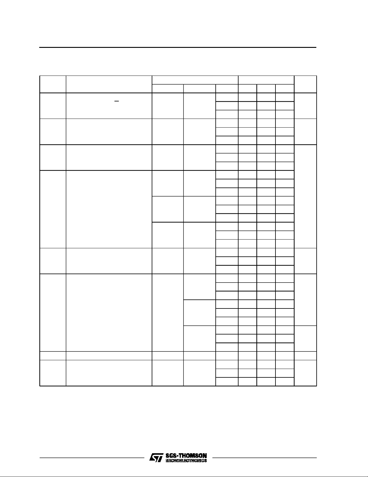
STATIC ELECTRICAL CHARACTERISTICS (over recommended operating conditions)
Test Conditions Value
Symbol Parameter
Quiescent
I
L
Current
HCC
Types
HCF
Types
V
OH
Output High
Voltage
V
OL
Output Low
Voltage
V
IH
Input High
Voltage
V
IL
Input Low
Voltage
OH
Output
Drive
Current
HCC
Types
I
HCF
Types
I
OL
Output
Sink
Current
HCC
Types
HCF
Types
I
IH,IIL
Input
Leakage
Current
HCC
Types
HCF
Types
Input Capacitance Any Input 5 7.5 pF
C
I
*T
=–55°C for HCC device : – 40°C for HCF device.
Low
*T
=+125°C for HCC device : + 85°C for HCF device.
High
TheNoiseMarginforboth ”1” and ”0” level is : 1V min.with VDD= 5V,2V min. withVDD=10V, 2.5 V min. withVDD= 15V.
V
V
O
|IO|V
I
(V) (V) (µA) (V)
T
DD
* 25°CT
Low
Min. Ma x. Min. Typ. Max . Min. Max.
0/ 5 5 1 0.02 1 30
0/10 10 2 0.02 2 60
0/15 15 4 0.02 4 120
0/20 20 20 0.04 20 600
0/ 5 5 4 0.02 4 30
0/10 10 8 0.02 8 60
0/15 15 16 0.02 16 120
0/ 5 < 1 5 4.95 4.95 4.95
0/10 < 1 10 9.95 9.95 9.95
0/15 < 1 15 14.95 14.95 14.95
5/0 < 1 5 0.05 0.05 0.05
10/0 < 1 10 0.05 0.05 0.05
15/0 < 1 15 0.05 0.05 0.05
0.5/4.5 < 1 5 3.5 3.5 3.5
1/9 < 1 10 7 7 7
1.5/13.5 < 1 15 11 11 11
4.5/0.5 < 1 5 1.5 1.5 1.5
9/1 < 1 10 3 3 3
13.5/1.5 < 1 15 4 4 4
0/ 5 2.5 5 – 2 – 1.6 – 3.2 – 1.15
0/ 5 4.6 5 – 0.64 – 0.51 – 1 – 0.36
0/10 9.5 10 – 1.6 – 1.3 – 2.6 – 0.9
0/15 13.5 15 – 4.2 – 3.4 – 6.8 – 2.4
0/ 5 2.5 5 – 1.53 – 1.36 – 3.2 – 1.1
0/ 5 4.6 5 – 0.52 – 0.44 – 1 – 0.36
0/10 9.5 10 – 1.3 – 1.1 – 2.6 – 0.9
0/15 13.5 15 – 3.6 – 3.0 – 6.8 – 2.4
0/ 5 0.4 5 0.64 0.51 1 0.36
0/10 0.5 10 1.6 1.3 2.6 0.9
0/15 1.5 15 4.2 3.4 6.8 2.4
0/ 5 0.4 5 0.52 0.44 1 0.36
0/10 0.5 10 1.3 1.1 2.6 0.9
0/15 1.5 15 3.6 3.0 6.8 2.4
–5
0/18
18 ± 0.1 ±10
± 0.1 ± 1
Any Input
0/15
15 ± 0.3 ±10
–5
± 0.3 ± 1
High
Unit
*
µA
V
V
V
V
mA
mA
µA
4/14
HCC/HCF4098B
DYNAMIC ELECTRICAL CHARACTERISTICS (T
=25°C, CL= 50pF, RL= 200kΩ,
amb
typical temperature coefficient for all VDDvalues is 0.3%/°C, all input rise and fall times = 20ns)
Symbol Parameter
t
PLH,tPHL
t
WH,tWL
Trigger Propagation Delay Time
(+ TR, – TR to Q, Q)
Trigger Pulse Width
5 to 10.000 ≥ 15
5 to 10.000 ≥ 15
t
TLH
Transition Time
5 to 10.000 ≥ 15
t
THL
Transition Time
5 to 10.000 15 to 10.000
5 to 10.000
5 to 10.000
t
PLH,tPHL
Propagation Delay Time (reset)
5 to 10.000 ≥ 15
t
R Pulse Width (reset)
W
t
(TR) Rise or Fall Time (trigger) 5 to 15 100 µs
r,tf
Pulse Width Match Between
Circuits in Same Package
Test Conditions Value
R
(kΩ) CX(pF) VDD(V) Min. Typ. Max.
X
5250500
10 125 250
15 100 200
5 140 70
10 60 30
15 40 20
5100200
10 50 100
15 40 80
5100200
10 50 100
15 40 80
5150300
0.01µF
to 0.1µF
10 75 150
15 65 130
5250500
0.1µF
to 1µF
10 150 300
15 80 160
5225450
10 125 250
15 75 150
5 200 100
15
10 80 40
15 60 30
51200600
100
1000
10 600 300
15 500 250
550250
0.1µF
10 30 15
15 20 10
5510
10 10.000
10 7.5 15
15 7.5 15
Unit
ns
ns
ns
ns
ns
µs
%
5/14

HCC/HCF4098B
Figure2 : TypicalOutput Low (sink)Current Charac-
teristics.
Figure4 :Typical Output High (source) Current Char-
acteristics.
Figure3 :Minimum Output Low(sink) Current Char-
acteristics.
Figure 5 : Minimum Output High (source) Current
Characteristics.
Figure6: TypicalPropagation Delay Times vs.Load
Capacitance, Trigger in to Q out. (All
values ofCXand Rx).
6/14
Figure 7 : Transition Time vs.Load Capacitance for
RX=5kΩ, 10000 kΩ and CX= 15pF,
10000pF.

HCC/HCF4098B
Figure 8 : Typical External Resistance vs. Pulse
WidthatVarious VDDand C
X.
Figure 10 : Typical Minimum Reset Pulse Width vs.
External Capacitance.
Figure 9 : Typical External Capacitance vs.Pulse
Width at Various VDDand R
X.
Figure 11 : Average Power Dissipation for100%DutyCycle vs.One-shot Pulsewidth.
To calculateaverage power dissipation
(P) for less than 100% duty cycle :
=average power for 100%duty cycle
P
100
τ
m
P=
τ
e.g. : Fortm … 600ms tT = 1000ms,
P=
1000
(seedottedlineon graph)
where τm=one-shot pulse width
P
100
T
τ
=trigger pulseperiod
T
=
CX= 0.01µF, V
600
103µW = 600µW
DD
=5V
7/14

HCC/HCF4098B
TEST CIRCUITS
Figure 12 : Quiescent -DeviceCurrent. Figure13 :Input-Voltage.
Figure 14 : Input Leakage.
8/14

TYPICAL APPLICATIONS
Figure 15 : Astable Multivibrator withRestart after Reset Capability.
R
IDD(Avg)
X
10kΩ
|
|
|
|
|
|
|
|
|
|
|
▼
10MΩ
Notes : All values are typical
1mA
0.05mA
2.5mA
0.5mA
5mA
1mA
CXrange : 0.0001µF to 0.1µF.
(T1 + T2)
↓
↓
↓
HCC/HCF4098B
T
X
3.8µs
↓
0.5s
3.2µs
↓
0.5s
3µs
↓
0.5s
V
5V
10V
15V
DD
Figure 16 : Pulse Delay.
9/14

HCC/HCF4098B
Plastic DIP16 (0.25) MECHANICAL DATA
DIM.
MIN. TYP. MAX. MIN. TYP. MAX.
a1 0.51 0.020
B 0.77 1.65 0.030 0.065
b 0.5 0.020
b1 0.25 0.010
D 20 0.787
E 8.5 0.335
e 2.54 0.100
e3 17.78 0.700
F 7.1 0.280
I 5.1 0.201
L 3.3 0.130
Z 1.27 0.050
mm inch
10/14
P001C

Ceramic DIP16/1 MECHANICAL DATA
HCC/HCF4098B
DIM.
MIN. TYP. MAX. MIN. TYP. MAX.
A 20 0.787
B 7 0.276
D 3.3 0.130
E 0.38 0.015
e3 17.78 0.700
F 2.29 2.79 0.090 0.110
G 0.4 0.55 0.016 0.022
H 1.17 1.52 0.046 0.060
L 0.22 0.31 0.009 0.012
M 0.51 1.27 0.020 0.050
N 10.3 0.406
P 7.8 8.05 0.307 0.317
Q 5.08 0.200
mm inch
P053D
11/14

HCC/HCF4098B
SO16 (Narrow) MECHANICAL DATA
DIM.
MIN. TYP. MAX. MIN. TYP. MAX.
A 1.75 0.068
a1 0.1 0.2 0.004 0.007
a2 1.65 0.064
b 0.35 0.46 0.013 0.018
b1 0.19 0.25 0.007 0.010
C 0.5 0.019
c1 45° (typ.)
D 9.8 10 0.385 0.393
E 5.8 6.2 0.228 0.244
e 1.27 0.050
e3 8.89 0.350
F 3.8 4.0 0.149 0.157
G 4.6 5.3 0.181 0.208
L 0.5 1.27 0.019 0.050
M 0.62 0.024
S8°(max.)
mm inch
12/14
P013H

PLCC20 MECHANICAL DATA
HCC/HCF4098B
DIM.
MIN. TYP. MAX. MIN. TYP. MAX.
A 9.78 10.03 0.385 0.395
B 8.89 9.04 0.350 0.356
D 4.2 4.57 0.165 0.180
d1 2.54 0.100
d2 0.56 0.022
E 7.37 8.38 0.290 0.330
e 1.27 0.050
e3 5.08 0.200
F 0.38 0.015
G 0.101 0.004
M 1.27 0.050
M1 1.14 0.045
mm inch
P027A
13/14

HCC/HCF4098B
Information furnished is believed tobe accurate and reliable. However, SGS-THOMSON Microelectronics assumes no responsability for the
consequences of use of such information nor for any infringementofpatents orother rights of third parties which may results from its use. No
license isgrantedby implication orotherwiseunder any patentorpatent rights ofSGS-THOMSONMicroelectronics. Specificationsmentioned
in this publication are subject to changewithout notice.This publication supersedes andreplaces all information previously supplied.
SGS-THOMSON Microelectronicsproductsare notauthorized foruse ascritical componentsin life supportdevices orsystemswithout express
written approval of SGS-THOMSON Microelectonics.
1994 SGS-THOMSON Microelectronics - All RightsReserved
Australia - Brazil - France - Germany - Hong Kong - Italy - Japan - Korea - Malaysia - Malta - Morocco - The Netherlands -
Singapore - Spain - Sweden - Switzerland - Taiwan - Thailand - UnitedKingdom - U.S.A
SGS-THOMSON MicroelectronicsGROUPOF COMPANIES
14/14
 Loading...