

8–STAGESHIFT-AND-STOREBUS REGISTER
.3-STATE PARALLEL OUTPUTS FOR CON-
NECTIONTO COMMON BUS
.SEPARATE SERIAL OUTPUTS SYN-
CHRONOUSTOBOTH POSITIVEANDNEGATIVE CLOCK EDGES FOR CASCADING
.MEDIUM SPEED OPERATION 5MHzAT 10V
.STANDARDIZED SYMMETRICAL OUTPUT
CHARACTERISTICS
.QUIESCENT CURRENT SPECIFIED TO 20V
FOR HCC DEVICE
.5V, 10V,AND 15VPARAMETRIC RATINGS
.INPUT CURRENTOF100nA AT18V AND 25°C
FOR HCC DEVICE
.100% TESTEDFOR QUIESCENTCURRENT
.MEETSALLREQUIREMENTSOFJEDECTEN-
TATIVE STANDARD N°. 13A, ”STANDARD
SPECIFICATIONS FOR DESCRIPTIONOF ”B”
SERIESCMOS DEVICES”
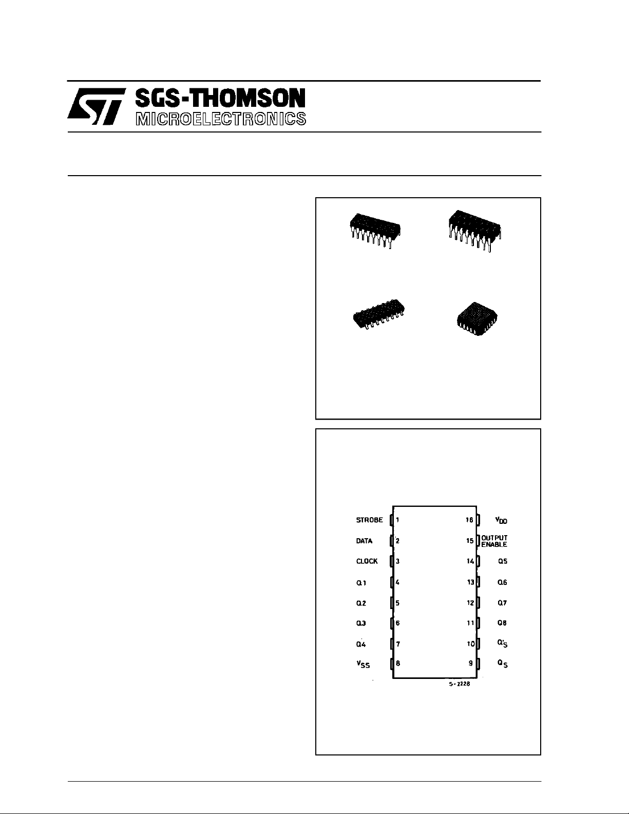
HCC/HCF4094B
EY
(Plastic Package)
M1
(MicroPackage)
ORDERCODES :
HCC4094BF HCF4094BM1
HCF4094BEY HCF4094BC1
(CeramicFritSeal Package)
F
C1
(PlasticChipCarrier)
DESCRIPTION
The HCC4094B (extended temperature range) and
HCF4094B (intermediate temperature range) are
monolithic integrated circuits available in 16-lead
dual in-line plastic or ceramic packageand plastic
micropackage.
The HCC/HCF4094B isan 8-stage serial shiftreg-
ister having a storage latch associated with each
stage for strobing data from the serial input to parallel buffered 3-state outputs. The parallel outputs
may be connected directly to common bus lines.
Dataisshiftedonpositive clocktransitions.The data
in each shift register stageistransferred to thestorage register when the STROBEinput is high. Data
in thestorage register appears atthe outputswhenever the OUTPUT-ENABLE signal is high.Twoserial outputsare available for cascading a numberof
HCC/HCF4094B devices. Data is available at the
QSserialoutput terminal onpositiveclock edges to
allowfor high-speed operation in cascaded systems
in whichthe clockrise time is fast.The sameserial
information,availableatthe Q’Sterminalon thenext
negative clock edge, provides a means for cascading HCC/HCF4094B devices when the clock rise
time isslow.
PIN CON NEC TI O NS
June 1989
1/14

HCC/HCF4094B
FUNCTIONAL DIAGRAM
ABSOLUTE MAXIMUM RATI NG S
Symbol Parameter Valu e Unit
V
* Supply Voltage :HCC Types
DD
HCF Types
V
Input Voltage – 0.5 to VDD+ 0.5 V
i
I
DC Input Current (any one input) ± 10 mA
I
P
Total Power Dissipation (per package)
tot
Dissipation per Output Transistor
for T
T
Operating Temperature : HCC Types
op
= Full Package-temperature Range
op
HCF Types
T
Stresses abovethose listedunder ”Absolute MaximumRatings”may cause permanent damage tothe device. This is a stressrating only and
functionaloperation of the deviceat these or any otherconditions abovethose indicated inthe operational sectionsof this specification is not
implied.Exposure toabsolutemaximum ratingconditions for external periodsmay affectdevice reliability.
*
Allvoltage valuesare referred to VSSpinvoltage.
Storage Temperature – 65 to + 150 °C
stg
– 0.5 to + 20
– 0.5 to + 18
200
100
–55to+125
–40to+85
V
V
mW
mW
°C
°C
RECOMMENDED OPERATING CONDITIONS
Symbol Parameter Value Unit
2/14
V
Supply Voltage : HC C Types
DD
HCF Types
V
Input Voltage 0 to V
I
T
Operating Temperature : HCC Types
op
HCF Types
3to18
3to15
DD
– 55 to + 125
–40to+85
V
V
V
°C
°C
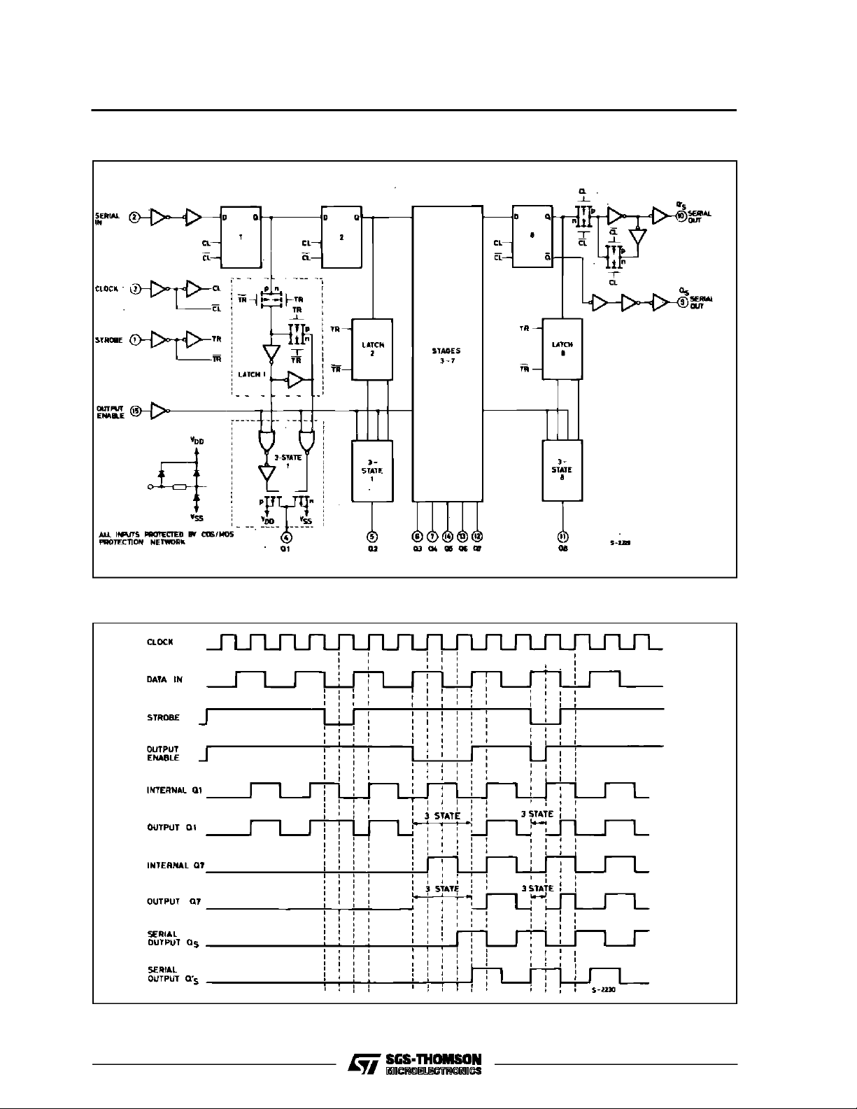
LOGIC DIAGRAMS
HCC/HCF4094B
TIMING DIAGRAM
3/14

HCC/HCF4094B
TRUTH TABLE
TRUTH TABLE
∆ Outputs
CL
–
/
–
–
\
–
–
/
–
–
/
–
–
/
–
–
\
–
▲= Level Change Logic1 ≡ High
X = Don’tCare Logic0 ≡ Low
NC = No Change
OC = Open Circuit
*
Atthe positiveclock edgeinformation in the 7th shiftregister stageis transferred to the 8th registerstage and the QSoutput.
Enable
0XXOCOCQ7NC
0XXOCOCNCQ7
1 0 X NCNCQ7NC
1100Q
1111Q
1 1 1 NCNCNCQ7
Strobe Dat a
Parallel Outputs Serial Outputs
Q1 QN QS* Q’S
-1 Q7 NC
N
-1 Q7 NC
N
4/14

HCC/HCF4094B
STATIC ELECTRICAL CHARACTERISTICS(over recommended operating conditions)
Test Conditions Value
T
V
Symbol Parameter
I
Quiescent
L
Current
HCC
Types
V
I
(V) (V) (µA) (V)
0/ 5 5 5 0.04 5 150
0/10 10 10 0.04 10 300
0/15 15 20 0.04 20 600
O
|IO|V
DD
Min. M ax. Min. Typ. M ax. Min. Max.
0/20 20 100 0.08 100 3000
HCF
Types
OH
Output High
V
Voltage
0/ 5 5 20 0.04 20 150
0/10 10 40 0.04 40 300
0/15 15 80 0.04 80 600
0/ 5 < 1 5 4.95 4.95 4.95
0/10 < 1 10 9.95 9.95 9.95
0/15 < 1 15 14.95 14.95 14.95
OL
Output Low
V
Voltage
5/0 < 1 5 0.05 0.05 0.05
10/0 < 1 10 0.05 0.05 0.05
15/0 < 1 15 0.05 0.05 0.05
IH
Input High
V
Voltage
0.5/4.5 < 1 5 3.5 3.5 3.5
1/9 < 1 10 7 7 7
1.5/13.5 < 1 15 11 11 11
IL
Input Low
V
Voltage
4.5/0.5 < 1 5 1.5 1.5 1.5
9/1 < 1 10 3 3 3
13.5/1.5 < 1 15 4 4 4
I
OH
Output
Drive
Current
HCC
Types
0/ 5 2.5 5 – 2 – 1.6 – 3.2 – 1.15
0/ 5 4.6 5 – 0.64 – 0.51 – 1 – 0.36
0/10 9.5 10 – 1.6 – 1.3 – 2.6 – 0.9
0/15 13.5 15 – 4.2 – 3.4 – 6.8 – 2.4
0/ 5 2.5 5 – 1.53 – 1.36 – 3.2 – 1.1
HCF
Types
0/ 5 4.6 5 – 0.52 – 0.44 – 1 – 0.36
0/10 9.5 10 – 1.3 – 1.1 – 2.6 – 0.9
0/15 13.5 15 – 3.6 – 3.0 – 6.8 – 2.4
OL
Output
Sink
Current
HCC
Types
I
HCF
Types
I
IH,IIL
Input
Leakage
Current
HCC
Types
HCF
Types
I
OH,IOL
*T
Low
*T
High
TheNoise Margin for both”1” and”0” levelis : 1V min. withVDD=5V, 2V min.withVDD= 10V,2.5V min. withVDD= 15V.
3-state
Output
Leakage
Current
Input Capacitance Any Input 5 7.5 pF
C
I
=–55°CforHCC device : – 40°C for HCFdevice.
= +125°C for HCC device: + 85°C for HCF device.
HCC
Types
HCF
Types
0/ 5 0.4 5 0.64 0.51 1 0.36
0/10 0.5 10 1.6 1.3 2.6 0.9
0/15 1.5 15 4.2 3.4 6.8 2.4
0/ 5 0.4 5 0.52 0.44 1 0.36
0/10 0.5 10 1.3 1.1 2.6 0.9
0/15 1.5 15 3.6 3.0 6.8 2.4
0/18
18 ± 0.1 ±10
Any Input
0/15
15 ± 0.3 ±10
0/18 0/18 18 ± 0.4 ± 10
0/15 0/15 15 ± 1.0 ± 10
* 25°CT
Low
–5
± 0.1 ± 1
–5
± 0.3 ± 1
-4
± 0.4 ± 12
-4
± 1.0 ± 7.5
High
*
Unit
µA
V
V
V
V
mA
mA
µA
µA
5/14

HCC/HCF4094B
DYNAMIC ELECTRICAL CHARACTERISTICS(T
=25°C, CL= 50pF,RL= 200kΩ,
amb
typical temperature coefficient for all VDD= 0.3%/°C values , all input rise and fall time = 20ns)
Symbol Parameter
t
PLH,tPHL
t
PLH,tPHL
t
PLH,tPHL
Propagation Delay Time Clock to
Serial Output Q
S
Propagation Delay Time Clock to
Serial Output Q’
S
Propagation Delay Time Clock to
Parallel Output
t
PLH,tPHL
Propagation Delay Time Strobe
to Parallel Output
t
PHZ
Propagation Delay Time Output
Enable to Parallel Output :
Output High to High Impedance
t
PL Z
t
t
t
se tu p
t
TL H,tTHL
t
r,tf
f
max
Out Low to High Impedance 5 225 450
Strobe Pulse Width 5 200 100
W
Clock Pulse Width 5 200 100
W
Data Setup Time 5 125 60
Transition Time 5 100 200
Clock Input Rise or Fall Time 5 15
Maximum Clock Input Frequency 5 1.25 2.5
Test Conditions Value
V
(V) Min. Typ. Max.
DD
5300600
10 125 250
15 95 190
5230460
10 110 220
15 75 150
5420840
10 195 390
15 135 270
5290580
10 145 290
15 100 200
5140280
10 75 150
15 55 110
10 95 190
15 70 140
10 80 40
15 70 35
10 100 50
15 83 40
10 55 30
15 35 20
10 50 100
15 40 80
10 5
15 5
10 2.5 5
15 3 6
Unit
ns
ns
ns
ns
ns
ns
ns
ns
ns
ns
µs
MHz
6/14

HCC/HCF4094B
TypicalOutputLow (sink)Current Characteristics. Minimum Output Low(sink) Current Charac-
teristics.
TypicalOutputHigh (source) Current Charateristics.
Clock-to-serial OutputQSPropagation Delay vs.
CL.
Minimum Output High(source)Current Characteristics.
Clock-to-serial Output Q’SPropagation Delay vs.
CL.
7/14

HCC/HCF4094B
Clock-to-parallel OutputPropagation Delay vs. CL. Strobe-to-parallel OutputPropagation Delayvs.CL.
OutputEnable-to-parallel Output Propagation
Delay vs.
TypicalMaximum-clock Frequency vs. Supply
Voltage.
TypicalTransition Timevs. LoadCapacitance.
Dynamic Power Dissipation vs. InputClock Frequency.
8/14

TYPICAL APPLICATION
REMOTECONTROL HOLDINGREGISTER
HCC/HCF4094B
TEST CIRCUITS
QuiescentDevice Current. Noise Immunity.
Input Leakage Current.
9/14

HCC/HCF4094B
Plastic DIP16 (0.25) MECHANICAL DATA
DIM.
MIN. TYP. MAX. MIN. TYP. MAX.
a1 0.51 0.020
B 0.77 1.65 0.030 0.065
b 0.5 0.020
b1 0.25 0.010
D 20 0.787
E 8.5 0.335
e 2.54 0.100
e3 17.78 0.700
F 7.1 0.280
I 5.1 0.201
L 3.3 0.130
Z 1.27 0.050
mm inch
10/14
P001C

Ceramic DIP16/1 MECHANICAL DATA
HCC/HCF4094B
DIM.
MIN. TYP. MAX. MIN. TYP. MAX.
A 20 0.787
B 7 0.276
D 3.3 0.130
E 0.38 0.015
e3 17.78 0.700
F 2.29 2.79 0.090 0.110
G 0.4 0.55 0.016 0.022
H 1.17 1.52 0.046 0.060
L 0.22 0.31 0.009 0.012
M 0.51 1.27 0.020 0.050
N 10.3 0.406
P 7.8 8.05 0.307 0.317
Q 5.08 0.200
mm inch
P053D
11/14

HCC/HCF4094B
SO16 (Narrow) MECHANICAL DATA
DIM.
MIN. TYP. MAX. MIN. TYP. MAX.
A 1.75 0.068
a1 0.1 0.2 0.004 0.007
a2 1.65 0.064
b 0.35 0.46 0.013 0.018
b1 0.19 0.25 0.007 0.010
C 0.5 0.019
c1 45° (typ.)
D 9.8 10 0.385 0.393
E 5.8 6.2 0.228 0.244
e 1.27 0.050
e3 8.89 0.350
F 3.8 4.0 0.149 0.157
G 4.6 5.3 0.181 0.208
L 0.5 1.27 0.019 0.050
M 0.62 0.024
S8°(max.)
mm inch
12/14
P013H

PLCC20 MECHANICAL DATA
HCC/HCF4094B
DIM.
MIN. TYP. MAX. MIN. TYP. MAX.
A 9.78 10.03 0.385 0.395
B 8.89 9.04 0.350 0.356
D 4.2 4.57 0.165 0.180
d1 2.54 0.100
d2 0.56 0.022
E 7.37 8.38 0.290 0.330
e 1.27 0.050
e3 5.08 0.200
F 0.38 0.015
G 0.101 0.004
M 1.27 0.050
M1 1.14 0.045
mm inch
P027A
13/14

HCC/HCF4094B
Information furnished is believed tobe accurate and reliable.However, SGS-THOMSON Microelectronicsassumes no responsability forthe
consequences of useof such information nor for any infringement of patents orother rights of third partieswhich may results from its use. No
license isgranted by implication or otherwise under any patent orpatent rights ofSGS-THOMSON Microelectronics. Specificationsmentioned
in this publication are subject to changewithout notice. This publication supersedesand replaces all information previously supplied.
SGS-THOMSON Microelectronicsproducts are not authorized foruse ascritical componentsin lifesupport devicesor systemswithout express
written approval of SGS-THOMSONMicroelectonics.
1994 SGS-THOMSON Microelectronics - All RightsReserved
Australia - Brazil - France - Germany- HongKong - Italy - Japan - Korea- Malaysia - Malta -Morocco - The Netherlands-
Singapore - Spain - Sweden - Switzerland - Taiwan - Thailand - UnitedKingdom - U.S.A
SGS-THOMSON Microelectronics GROUP OF COMPANIES
14/14
 Loading...