

Datasheet HCF4093BM1, HCF4093BEY, HCF4093BC1, HCC4093BF Datasheet (SGS Thomson Microelectronics)
QUAD 2-INPUT NAND SCHMIDT TRIGGERS
.SCHMITT-TRIGGERACTIONONEACHINPUT
WITH NOEXTERNAL COMPONENTS
.HYSTERESIS VOLTAGE TYPICALLY 0.9V AT
VDD=5V AND 2.3VAT VDD= 10V
.NOISE IMMUNITY GREATER THAN 50% OF
VDD(typ.)
.NO LIMIT ON INPUTRISEAND FALL TIMES
.STANDARDIZED SYMMETRICAL OUTPUT
CHARACTERISTICS
.QUIESCENT CURRENT SPECIFIED TO 20V
FOR HCC DEVICE
.5V, 10V, AND 15V PARAMETRIC RATINGS
.INPUT CURRENT OF 100nA AT 18V AND
25°C FORHCC DEVICE
.100% TESTEDFOR QUIESCENTCURRENT
.MEETSALLREQUIREMENTSOFJEDECTEN-
TATIVE STANDARD N°. 13A, ”STANDARD
SPECIFICATIONS FOR DESCRIPTION OF ”B”
SERIESCMOS DEVICES”
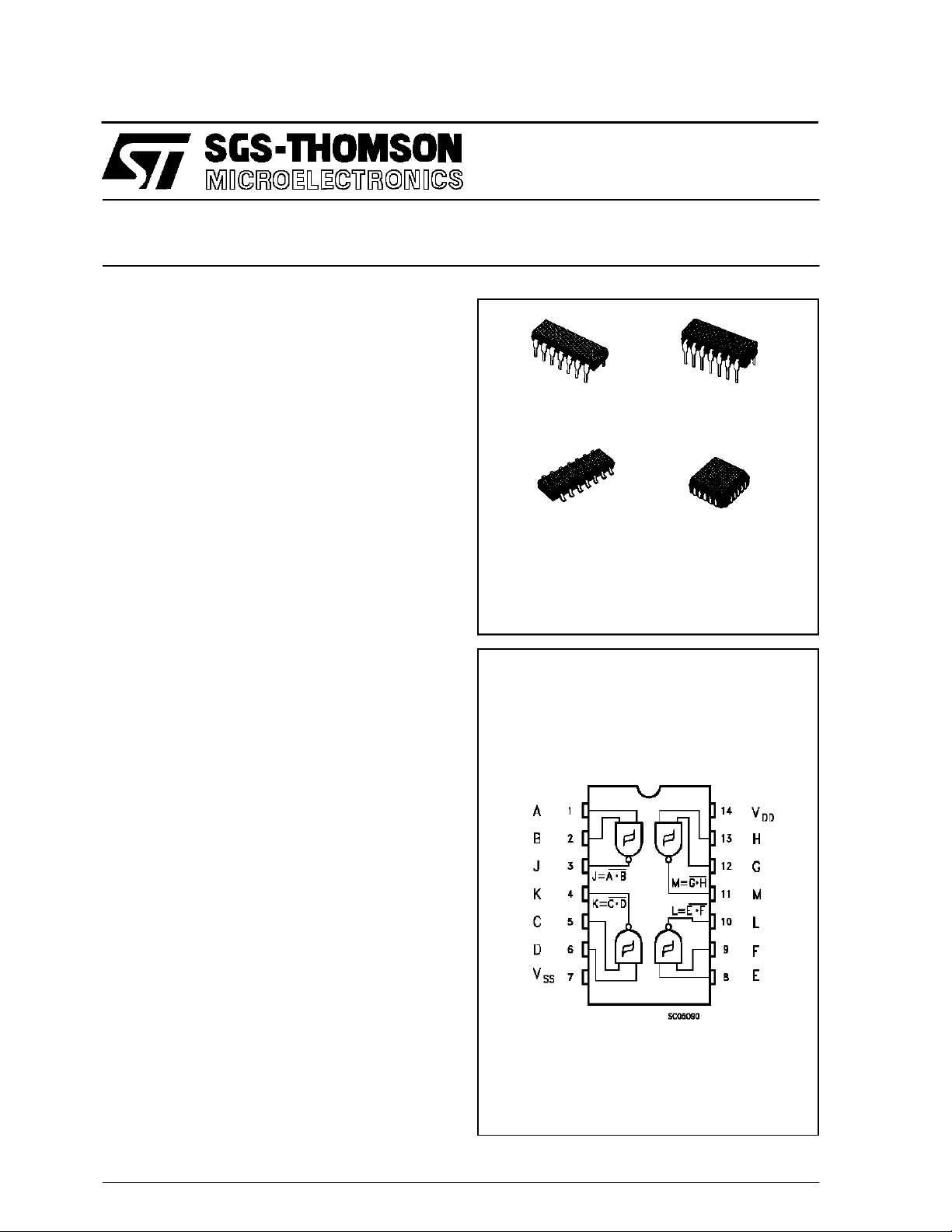
HCC/HCF4093B
EY
(Plastic Package)F(Ceramic Frit Seal Package)
M1
(MicroPackage)
ORDERCODES :
HCC4093BF HCF4093BM1
HCF4093BEY HCF4093BC1
(Plastic Chip Carrier)
C1
DESCRIPTION
TheHCC4093B(extended temperature range) and
HCF4093B (intermediate temperature range) are
available in 14-lead dual in-line plastic or ceramic
package and plastic micropackage. The
HCC/HCF4093BconsistsoffourSchmitt-triggercircuits. Each circuit functions as a two-input NAND
gate withSchmitt-trigger actionon both inputs. The
gate switches at different points for positive and negative-going signals.
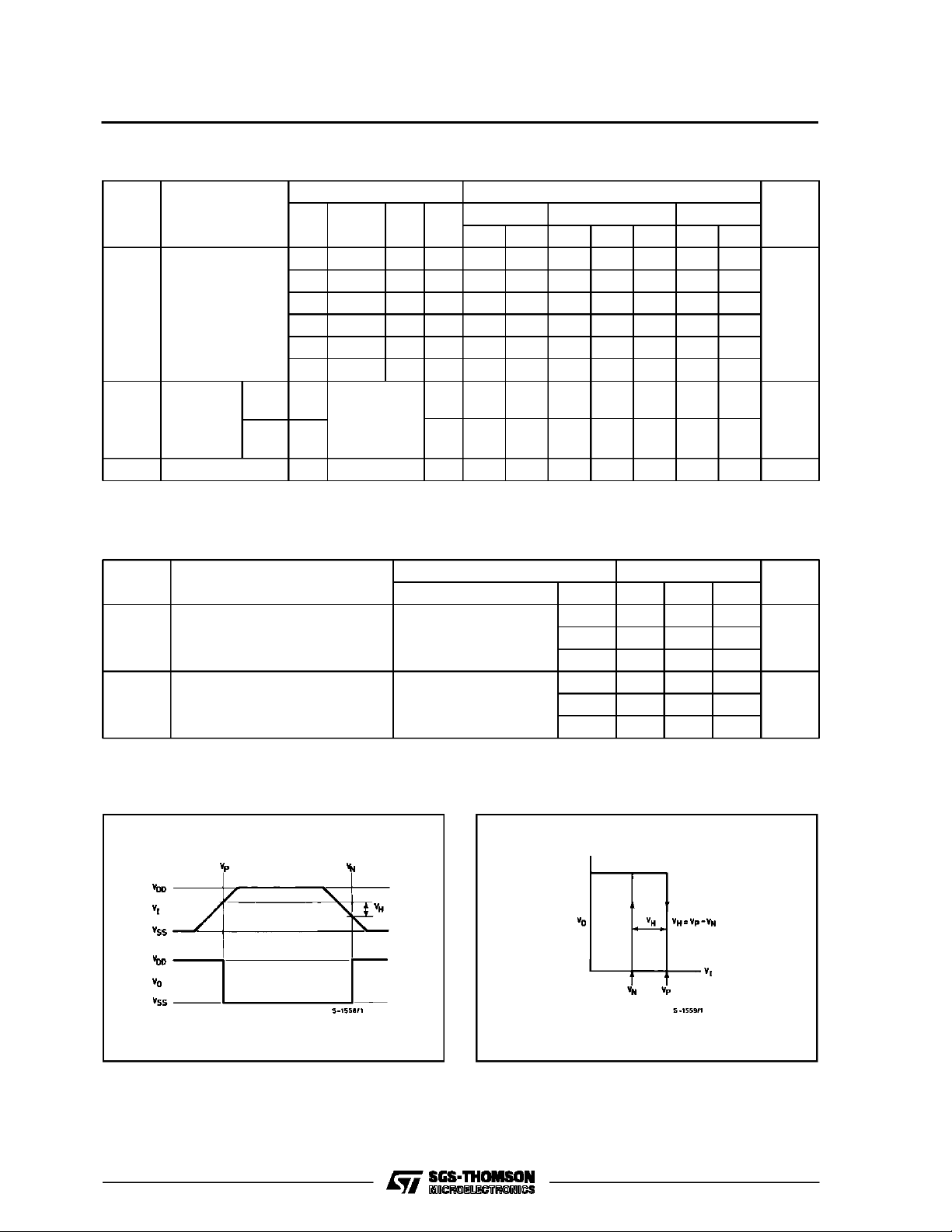
The difference between the positive voltage (VP)
and the negative voltage (VN) is defined as hysteresisvoltage (VH) (see fig.1).
PIN CO N NEC TI O NS
June 1989
1/13
HCC/HCF4093B
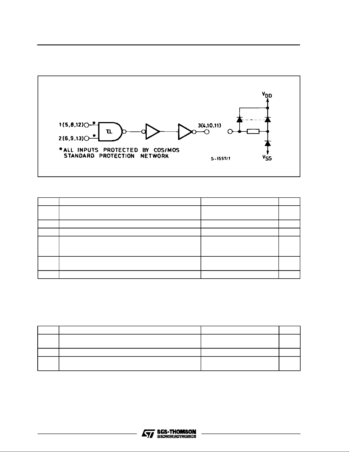
FUNCTIONAL DIAGRAM
1 of 4 Schmitt triggers
ABSOLUTE M AX IMU M RATI NG S
Symbol Parameter Val ue Unit
V
* Supply Voltage :HC C Types
DD
HCF Types
V
Input Voltage – 0.5 to VDD+ 0.5 V
I
I
DC Input Current (any one input) ± 10 mA
I
P
Total Power Dissipation (per package)
tot
Dissipation per Output Transistor
for T
T
Operating Temperature : HCC Types
op
= Full Package-temperature Range
op
HCF Types
T
Stresses above those listed under ”Absolute Maximum Ratings ”may cause permanent damage to the device. This is a stress
rating only and functional operation of the device at these or any other conditions above those indicated in the operational sections of this specification is not implied. Exposure to absolute maximum rating conditions for external periods may affect device
reliability.
* All voltage values are referred to VSSpin voltage.
Storage Temperature – 65 to + 150 °C
stg
– 0.5 to + 20
– 0.5 to + 18
200
100
–55to+125
–40to+85
V
V
mW
mW
°C
°C
RECOMMENDED OPERATING CONDITIONS
Symbol Parameter Value Unit
V
T
2/13
Supply Voltage : HC C Types
DD
HCF Types
V
Input Voltage 0 to V
I
Operating Temperature : HCC Types
op
HCF Types
3to18
3to15
DD
– 55 to + 125
–40to+85
V
V
V
°C
°C
HCC/HCF4093B
STATIC ELECTRICAL CHARACTERISTICS (over recommended operating conditions)
Test Conditions Value
V
Symbol Parameter
V
I
O
|IO|V
(V) (V) (µA) (V)
I
L
Quiescent
Current
HCC
Types
0/ 5 5 1 0.02 1 30
0/10 10 2 0.02 2 60
0/15 15 4 0.02 4 120
0/20 20 20 0.04 20 600
HCF
Types
V
Positive Trigger
P
Threshold Voltage
0/ 5 5 4 0.02 4 30
0/10 10 8 0.02 8 60
0/15 15 16 0.02 16 120
a 5 2.2 3.6 2.2 2.9 3.6 2.2 3.6
a 10 4.6 7.1 4.6 5.9 7.1 4.6 7.1
a 15 6.8 10.8 6.8 8.8 10.8 6.8 10.8
b 5 2.6 4 2.6 3.3 4 2.6 4
b 10 5.6 8.2 5.6 7 8.2 5.6 8.2
b 15 6.3 12.7 6.3 9.4 12.7 6.3 12.7
V
Negative Trigger
N
Threshold Voltage
a 5 0.9 2.8 0.9 1.9 2.8 0.9 2.8
a 10 2.5 5.2 2.5 3.9 5.2 2.5 5.2
a 15 4 7.4 4 5.8 7.4 4 7.4
b 5 1.4 3.2 1.4 2.3 3.2 1.4 3.2
b 10 3.4 6.6 3.4 5.1 6.6 3.4 6.6
b 15 4.8 9.6 4.8 7.3 9.6 4.8 9.6
V
Hysteresis Voltage a 5 0.3 1.6 0.3 0.9 1.6 0.3 1.6
H
a 10 1.2 3.4 1.2 2.3 3.4 1.2 3.4
a 15 1.6 5 1.6 3.5 5 1.6 5
b 5 0.3 1.6 0.3 0.9 1.6 0.3 1.6
b 10 1.2 3.4 1.2 2.3 3.4 1.2 3.4
b 15 1.6 5 1.6 3.5 5 1.6 5
OH
Output High
V
Voltage
0/ 5 < 1 5 4.95 4.95 4.95
0/10 < 1 10 9.95 9.95 9.95
0/15 < 1 15 14.95 14.95 14.95
OL
Output Low
V
Voltage
5/0 < 1 5 0.05 0.05 0.05
10/0 < 1 10 0.05 0.05 0.05
15/0 < 1 15 0.05 0.05 0.05
OH
Output
Drive
Current
HCC
Types
I
0/ 5 2.5 5 – 2 – 1.6 – 3.2 – 1.15
0/ 5 4.6 5 – 0.64 – 0.51 – 1 – 0.36
0/10 9.5 10 – 1.6 – 1.3 – 2.6 – 0.9
0/15 13.5 15 – 4.2 – 3.4 – 6.8 – 2.4
0/ 5 2.5 5 – 1.53 – 1.36 – 3.2 – 1.1
HCF
Types
0/ 5 4.6 5 – 0.52 – 0.44 – 1 – 0.36
0/10 9.5 10 – 1.3 – 1.1 – 2.6 – 0.9
0/15 13.5 15 – 3.6 – 3.0 – 6.8 – 2.4
a : input on terminals 1, 5, 8, 12 or 2, 6, 9, 13 ; other inputs to VDD.
b : input on terminals 1 and 2, 5 and 6, 8 and 9, or 12 and 13 ; other inputs to VDD.
*T
=–55°CforHCC device : -40°Cfor HCF device.
Low
*T
= +125°CforHCC device : +85°C for HCF device.
High
T
DD
* 25°CT
Low
Min. Max. Min. Typ. Max. Min. Max.
High
*
Unit
µA
V
V
V
V
V
mA
3/13
HCC/HCF4093B
STATIC ELECTRICAL CHARACTERISTICS( continued)
Test Conditions Valu e
Symbol Parameter
I
OL
Output
Sink
Current
I
IH,IIL
Input
Leakage
Current
HCC
Types
HCF
Types
Input Capacitance Any Input 5 7.5 pF
C
I
V
V
O
|IO|V
I
(V) (V) (µA) (V)
T
DD
Low
Min. Ma x. Min. Typ. Max. Min. Max.
0/ 5 0.4 5 0.64 0.51 1 0.36
0/10 0.5 10 1.6 1.3 2.6 0.9
0/15 1.5 15 4.2 3.4 6.8 2.4
0/ 5 0.4 5 0.52 0.44 1 0.36
0/10 0.5 10 1.3 1.1 2.6 0.9
0/15 1.5 15 3.6 3.0 6.8 2.4
0/18
18 ± 0.1 ± 10
Any Input
0/15
15 ± 0.3 ± 10
* 25°CT
-5
± 0.1 ± 1
-5
± 0.3 ± 1
High
*
Unit
mA
µA
DYNAMIC ELECTRICAL CHARACTERISTICS (T
=25°C, CL= 50pF, RL= 200kΩ,
amb
typical temperature coefficient for all VDD= 0.3%/°C values , all input rise and fall time = 20ns)
Symbol Parameter
t
PLH,tPHL
t
TL H,tTHL
Propagation Delay Time 5 190 380
Transition Time 5 100 200
Test Conditions
V
(V) Min. Typ . Max.
DD
10 90 180
15 65 130
10 50 100
15 40 80
Value
Figure1 : HysteresisDefinition, Characteristics and TestSetup.
(a) Definition of VP,VNand V
H
(b) Transfer characteristics of 1of 4 gates
Unit
ns
ns
4/13

HCC/HCF4093B
(c) Test setup Figure2 : Inputand OutputCharacteristics.
Figure 3 : Typical Current and Voltage TransferCharacteristics.
Figure 4 : Typical Voltage Transfer Characteristics as a Function of Temperature, and Test Circuit.
5/13

HCC/HCF4093B
Figure 5 : TypicalOutput Low (sink) Current Char-
acteristics.
Figure 7 : Typical Output High (source) Current
Characteristic.
Figure6 :MinimumOutputLow(sink)CurrentCharacteristics.
Figure 8 : Minimum Output High Current Characteristics.
Figure9 :TypicalPropagation Delay Time vs. Supply Voltage.
6/13
Figure10 :TypicalTransitionTimevs.LoadCapacitance.

HCC/HCF4093B
Figure 11 : Typical Trigger Threshold Voltage
vs.V
DD
Figure 12 : Typical per cent Hysteresis vs. Supply
Voltage.
Figure 13 : Typical Dissipation Characteristics. Figure 14 : Power Dissipation vs. Rise and Fall
Times.
7/13

HCC/HCF4093B
APPLICATIONS
Figure 15 : Wave Shaper. Figure16 :Monostable Multivibrator.
Figure17: AstableMultivibrator.
TEST CIRCUITS
Figure18: QuiescentDeviceCurrent.
8/13
Figure19 : Input Leakage Current.

Plastic DIP14 MECHANICAL DATA
HCC/HCF4093B
DIM.
MIN. TYP. MAX. MIN. TYP. MAX.
a1 0.51 0.020
B 1.39 1.65 0.055 0.065
b 0.5 0.020
b1 0.25 0.010
D 20 0.787
E 8.5 0.335
e 2.54 0.100
e3 15.24 0.600
F 7.1 0.280
I 5.1 0.201
L 3.3 0.130
Z 1.27 2.54 0.050 0.100
mm inch
P001A
9/13

HCC/HCF4093B
Ceramic DIP14/1 MECHANICAL DATA
DIM.
MIN. TYP. MAX. MIN. TYP. MAX.
A 20 0.787
B 7.0 0.276
D 3.3 0.130
E 0.38 0.015
e3 15.24 0.600
F 2.29 2.79 0.090 0.110
G 0.4 0.55 0.016 0.022
H 1.17 1.52 0.046 0.060
L 0.22 0.31 0.009 0.012
M 1.52 2.54 0.060 0.100
N 10.3 0.406
P 7.8 8.05 0.307 0.317
Q 5.08 0.200
mm inch
10/13
P053C

SO14 MECHANICAL DATA
HCC/HCF4093B
DIM.
MIN. TYP. MAX. MIN. TYP. MAX.
A 1.75 0.068
a1 0.1 0.2 0.003 0.007
a2 1.65 0.064
b 0.35 0.46 0.013 0.018
b1 0.19 0.25 0.007 0.010
C 0.5 0.019
c1 45° (typ.)
D 8.55 8.75 0.336 0.344
E 5.8 6.2 0.228 0.244
e 1.27 0.050
e3 7.62 0.300
F 3.8 4.0 0.149 0.157
G 4.6 5.3 0.181 0.208
L 0.5 1.27 0.019 0.050
M 0.68 0.026
S8°(max.)
mm inch
P013G
11/13

HCC/HCF4093B
PLCC20 MECHANICAL DATA
DIM.
MIN. TYP. MAX. MIN. TYP. MAX.
A 9.78 10.03 0.385 0.395
B 8.89 9.04 0.350 0.356
D 4.2 4.57 0.165 0.180
d1 2.54 0.100
d2 0.56 0.022
E 7.37 8.38 0.290 0.330
e 1.27 0.050
e3 5.08 0.200
F 0.38 0.015
G 0.101 0.004
M 1.27 0.050
M1 1.14 0.045
mm inch
12/13
P027A

HCC/HCF4093B
Information furnished is believed to be accurate and reliable.However, SGS-THOMSON Microelectronics assumes no responsability for the
consequences of use of such information nor for any infringementofpatents or other rights of third parties which may results from its use. No
license isgrantedby implication orotherwiseunder any patentorpatent rights ofSGS-THOMSONMicroelectronics. Specificationsmentioned
in this publication are subject to changewithout notice. This publication supersedes and replaces all information previously supplied.
SGS-THOMSON Microelectronicsproductsare notauthorized foruse ascritical componentsin life supportdevices orsystemswithout express
written approval of SGS-THOMSON Microelectonics.
1994 SGS-THOMSON Microelectronics - All RightsReserved
Australia - Brazil - France - Germany - Hong Kong - Italy - Japan - Korea - Malaysia - Malta - Morocco - The Netherlands -
Singapore - Spain - Sweden - Switzerland - Taiwan - Thailand - United Kingdom - U.S.A
SGS-THOMSON MicroelectronicsGROUPOF COMPANIES
13/13
 Loading...