

Datasheet HCF4077BM1, HCF4077BF, HCF4077BEY, HCF4077BC1, HCF4077B Datasheet (SGS Thomson Microelectronics)
...
4070B–QUAD EXCLUSIVE–OR GATE
4037B–QUAD EXCLUSIVE–NOR GATE
. MEDIUM-SPEED OPERATION t
70ns (typ.) AT VCC= 10V, CL= 50pF
PHL=tPLH
.QUIESCENT CURRENT SPECIFIED TO 20V
FOR HCC DEVICE
.5V, 10V AND 15VPARAMETRIC RATING
.INPUT CURRENT OF 100nA AT 18V AND
25°C FOR HCC DEVICE
.100% TESTEDFOR QUIESCENTCURRENT
.MEETSALLREQUIREMENTSOFJEDECTEN-
TATIVE STANDARD No. 13A, ”STANDARD
SPECIFICATIONS FOR DESCRIPTIONOF ”B”
SERIESCMOS DEVICES”
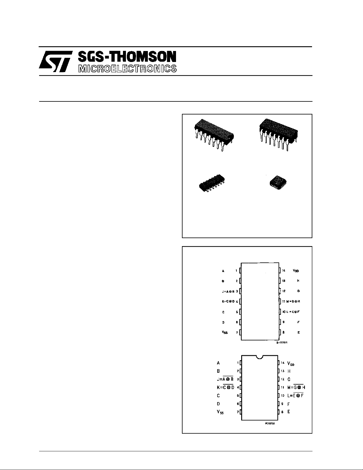
HCC4 07 0/7 7B
HCF4070/77B
GATES
=
EY
(PlasticPackage)
M1
(MicroPackage)
(CeramicPackage)
F
C1
(Chip Carrier)
DESCRIPTION
The HCC4070B/4077B (extended temperature
range) and HCF4070B/4077B (intermediate tem-
perature range) are monolithic integrated circuits,
available in 14-lead dual in-line plastic or ceramic
package and plasticmicropackage.
TheHCC/HCF4070Bcontains fourindependent ex-
clusive-ORgates.
TheHCC/HCF4077Bcontains fourindependent ex-
clusive-NOR gates.
TheHCC/HCF4070B andHCC/HCF4077Bprovide
the system designer with a means for direct implementation of the exclusive-OR and exclusiveNOR function, respectively. For applications as
Logical comparators, Adders/subtractors, Parity generatorsand checkers.
HCC4 0XX BF HCF40XXBM 1
ORDER CODES :
HCF40XXBEY HCF40XXBC1
PIN CONNECTIONS
4070B
4077B
September 1988
1/11

HCC/HCF4070B/4077B
FUN CTIONAL DIAG R A M
4070B 4077B
ABSOLU TE MAXIMUM RATING
Symbol Parameter Value Unit
* Supply Voltage: HCC Types
V
DD
HCF Types
V
P
Input Voltage -0.5 to VDD+ 0.5 V
i
I
DC Input Current (any one input) ± 10 mA
I
Total Power Dissipation (per package)
tot
Dissipation per Output Transistor
for Top = Full Package Temperature Range
T
Operating Temperature: HCC Types
op
HCF Types
T
Stressesabove those listedunder”AbsoluteMaximum Ratings”maycausepermanent damagetothedevice.Thisisastressratingonlyand functional
operation of the device at these or any otherconditions above thoseindicated in theoperational sections of thisspecificationisnotimplied.Exposure
to absolute maximum ratingconditionsforexternal periods mayaffect device reliability.
* All voltagevalues are referred to VSSpinvoltage.
Storage Temperature -65 to +150
stg
-0.5 to +20
-0.5 to +18
200
100
-55 to +125
-40 to +85
V
V
mW
mW
o
C
o
C
o
C
RECO MM ENDED OPERAT IN G C ONDITIO NS
Symbol Parameter Value Unit
V
Supply Voltage: HCC Types
DD
HCF Types
V
T
Input Voltage 0 to V
I
Operating Temperature: HCC Types
op
HCF Types
3to18
3to15
DD
-55 to +125
-40 to +85
TRUTH TABLES (1 of 4 gates)
2/11
HCC4070B
ABJ
000
101
011
110
ABJ
001
100
010
111
HCC4077B
V
V
V
o
C
o
C
HCC/HCF4070B/4077B
STATI C ELECTRICAL CHARACTE R ISTI CS (over rec ommended o peratin g conditi ons)
Test Conditios Value
Symbol Parameter
Quiescent
I
L
Current
HCC
Types
V
(V)
V
I
(V)
|IO|
(µA)
V
(V)
O
T
DD
*25
LOW
Min. Max. Min. Typ. Max. Min. Max.
0/5 5 1 0.02 1 30
0/10 10 2 0.02 2 60
0/15 15 4 0.02 4 120
o
CT
0/20 20 20 0.04 20 600
HCF
Types
0/5 5 4 0.02 4 30
0/10 10 8 0.02 8 60
0/15 15 16 0.02 16 120
OH
Output High
V
Voltage
0/5 < 1 5 4.95 4.95 4.95
0/10 < 1 10 9.95 9.95 9.95
0/15 < 1 15 14.95 14.95 14.95
OL
Output Low
V
Voltage
5/0 < 1 5 0.05 0.05 0.05
10/0 < 1 10 0.05 0.05 0.05
15/0 < 1 15 0.05 0.05 0.05
IH
Input High
V
Voltage
0.5/4.5 < 1 5 3.5 3.5 3.5
1/9 < 1 10 7 7 7
1.5/13.5 < 1 15 11 11 11
IL
Input Low
V
Voltage
4.5/0.5 < 1 5 1.5 1.5 1.5
9/1 < 1 10 3 3 3
13.5/1.5 < 1 15 4 4 4
OL
Output
Drive
Current
HCC
Types
I
0/5 2.5 5 -2 -1.6 -3.2 -1.15
0/5 4.6 5 -0.64 -0.51 -1 -0.36
0/10 9.5 10 -1.6 -1.3 -2.6 -0.9
0/15 13.5 15 -4.2 -3.4 -6.8 -2.4
0/5 2.5 5 -1.53 -1.36 -3.2 -1.1
HCF
Types
0/5 4.6 5 -0.52 -0.44 -1 -0.36
0/10 9.5 10 -1.3 -1.1 -2.6 -0.9
0/15 13.5 15 -3.6 -3.0 -6.8 -2.4
I
OL
Output
Sink
Current
HCC
Types
HCF
Types
0/5 0.4 5 0.64 0.51 1 0.36
0/10 0.5 10 1.6 1.3 2.6 0.9
0/15 1.5 15 4.2 3.4 6.8 2.4
0/5 0.4 5 0.52 0.44 1 0.36
0/10 0.5 10 1.3 1.1 2.6 0.9
0/15 1.5 15 3.6 3.0 6.8 2.4
I
IH,IIL
Input
Leakage
Current
C
*T
LOW
*T
HIGH
TheNoiseMarginfor both ”1” and”0”level is: 1V min. withVDD=5V,2 V min.withVDD=10V,2.5 V min. withVDD=15V
Input Capacitance Any Input 5 7.5 pF
I
=-55oCforHCC device:-40oC for HCF device.
=+125oCfor HCCdevice:+85oC for HCF device.
HCC
Types
HCF
Types
0/18
18 ±0.1 ±10
Any Input
0/15 15 ±0.3 ±10
-5
±0.1 ±1
-5
±0.3 ±1
HIGH
Unit
*
µA
V
V
V
V
mA
mA
µA
3/11
HCC/HCF4070B/4077B
DYNAMIC ELECTRICAL CHARACTERISTICS (T
=25oC, CL=50pF,RL= 200 KΩ,
amb
typic al temperature coeff ic ent for all VDDvalues is 03 %/oC, all input rise and fall ti mes = 20 ns)
Symbol Parameter
t
t
t
t
PLH
PHL
TLH
THL
Propagation Delay Time 5 140 280
Transition Time 5 100 200
Minimum Output High(source) Current Charac-
Test Conditions Value
V
(V) Min. Typ. Max.
DD
10 65 130
15 50 100
10 50 100
15 40 80
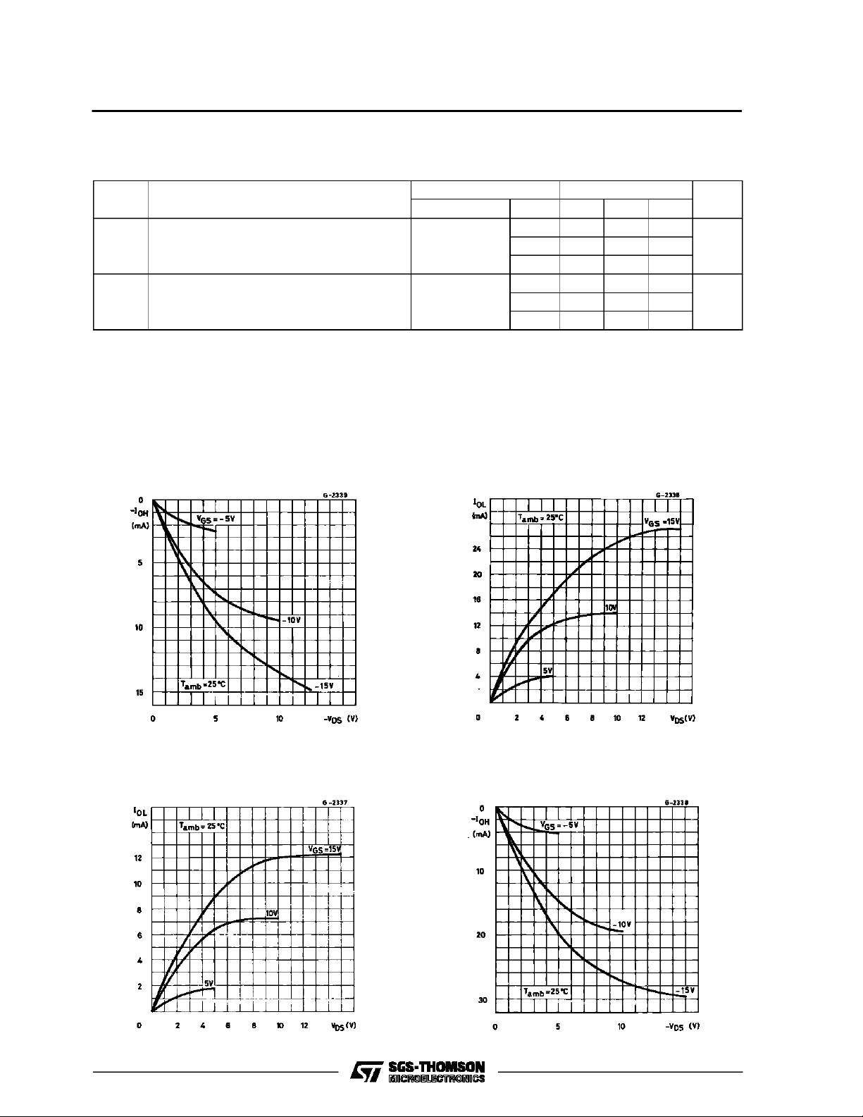
TypicalOutput Low (sink)Current.
Unit
ns
ns
teristics.
Minimum Output Low (sink)Current Characteristics.
4/11
TypicalOutput High (source) Current Characteristics.

HCC/HCF4070B/4077B
TypicalTransition Time vs. Load Capacitance. Typical Proagation Delay Time vs. Load Capacit-
ance.
TypicalPropagation Delay Time vs. Supply Voltage.
TypicalDynamic Power Dissipation vs.Input Frequency.
5/11

HCC/HCF4070B/4077B
TEST CIRCUIT
QuiescentDevice Current. Input Voltage.
Input Leakage Current.
6/11

Plastic DIP14 MECHANICALDATA
HCC/HCF4070B/4077B
DIM.
MIN. TYP. MAX. MIN. TYP. MAX.
a1 0.51 0.020
B 1.39 1.65 0.055 0.065
b 0.5 0.020
b1 0.25 0.010
D 20 0.787
E 8.5 0.335
e 2.54 0.100
e3 15.24 0.600
F 7.1 0.280
I 5.1 0.201
L 3.3 0.130
Z 1.27 2.54 0.050 0.100
mm inch
P001A
7/11

HCC/HCF4070B/4077B
Ceramic DIP14/1 MECHANICAL DATA
DIM.
MIN. TYP. MAX. MIN. TYP. MAX.
A 20 0.787
B 7.0 0.276
D 3.3 0.130
E 0.38 0.015
e3 15.24 0.600
F 2.29 2.79 0.090 0.110
G 0.4 0.55 0.016 0.022
H 1.17 1.52 0.046 0.060
L 0.22 0.31 0.009 0.012
M 1.52 2.54 0.060 0.100
N 10.3 0.406
P 7.8 8.05 0.307 0.317
Q 5.08 0.200
mm inch
8/11
P053C

SO14 MECHANICAL DATA
HCC/HCF4070B/4077B
DIM.
MIN. TYP. MAX. MIN. TYP. MAX.
A 1.75 0.068
a1 0.1 0.2 0.003 0.007
a2 1.65 0.064
b 0.35 0.46 0.013 0.018
b1 0.19 0.25 0.007 0.010
C 0.5 0.019
c1 45° (typ.)
D 8.55 8.75 0.336 0.344
E 5.8 6.2 0.228 0.244
e 1.27 0.050
e3 7.62 0.300
F 3.8 4.0 0.149 0.157
G 4.6 5.3 0.181 0.208
L 0.5 1.27 0.019 0.050
M 0.68 0.026
S8°(max.)
mm inch
P013G
9/11

HCC/HCF4070B/4077B
PLCC20 MECHANICAL DATA
DIM.
MIN. TYP. MAX. MIN. TYP. MAX.
A 9.78 10.03 0.385 0.395
B 8.89 9.04 0.350 0.356
D 4.2 4.57 0.165 0.180
d1 2.54 0.100
d2 0.56 0.022
E 7.37 8.38 0.290 0.330
e 1.27 0.050
e3 5.08 0.200
F 0.38 0.015
G 0.101 0.004
M 1.27 0.050
M1 1.14 0.045
mm inch
10/11
P027A

HCC/HCF4070B/4077B
Information furnished is believed to be accurate and reliable. However, SGS-THOMSON Microelectronics assumes no responsability forthe
consequences of use of such information nor for any infringement of patents or other rights of third parties which may results from its use. No
license is granted byimplicationor otherwise under any patentor patent rights ofSGS-THOMSON Microelectronics. Specificationsmentioned
in this publication aresubject to changewithout notice. This publication supersedes and replaces all information previously supplied.
SGS-THOMSON Microelectronicsproductsarenotauthorizedforuse ascriticalcomponentsinlifesupportdevicesorsystemswithoutexpress
written approval of SGS-THOMSON Microelectonics.
1994 SGS-THOMSON Microelectronics- All RightsReserved
Australia - Brazil - France - Germany - Hong Kong - Italy - Japan - Korea - Malaysia - Malta - Morocco - The Netherlands-
Singapore -Spain - Sweden - Switzerland - Taiwan - Thailand - UnitedKingdom - U.S.A
SGS-THOMSON Microelectronics GROUP OF COMPANIES
11/11
 Loading...