

.THREE STATE OUTPUTS
.INPUT DISABLE WITHOUT GATING THE
CLOCK
.GATED OUTPUT CONTROL LINES FOR EN-
ABLINGOR DISABLING THE OUTPUTS
.QUIESCENT CURRENT SPECIFIED TO 20V
FOR HCC DEVICE
.5V, 10V AND 15VPARAMETRIC RATINGS
.INPUT CURRENTOF 100nAAT 18V AND25
FOR HCC DEVICE
o
.100% TESTEDFOR QUIESCENTCURRENT
.MEETSALLREQUIREMENTSOFJEDECTEN-
TATIVE STANDARD N. 13A, ” STANDARD
SPECIFICATIONS FOR DESCRIPTION OF B
SERIESCMOS DEVICES ”
HCC4076B
HCF4076B
4 BIT D TYPE REGISTERS
EY
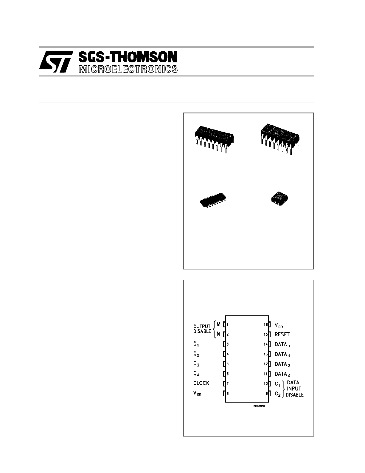
C
(PlasticPackage)
M1
(MicroPackage)
(CeramicPackage)
F
C1
(Chip Carrier)
DESCRIPTION
TheHCC4076B (extended temperature range) and
HCC4076B (intermediate temperature range) are
monolithic integrated circuit, available in 16 lead
dual in line plastic or ceramic package and plastic
micropackage.
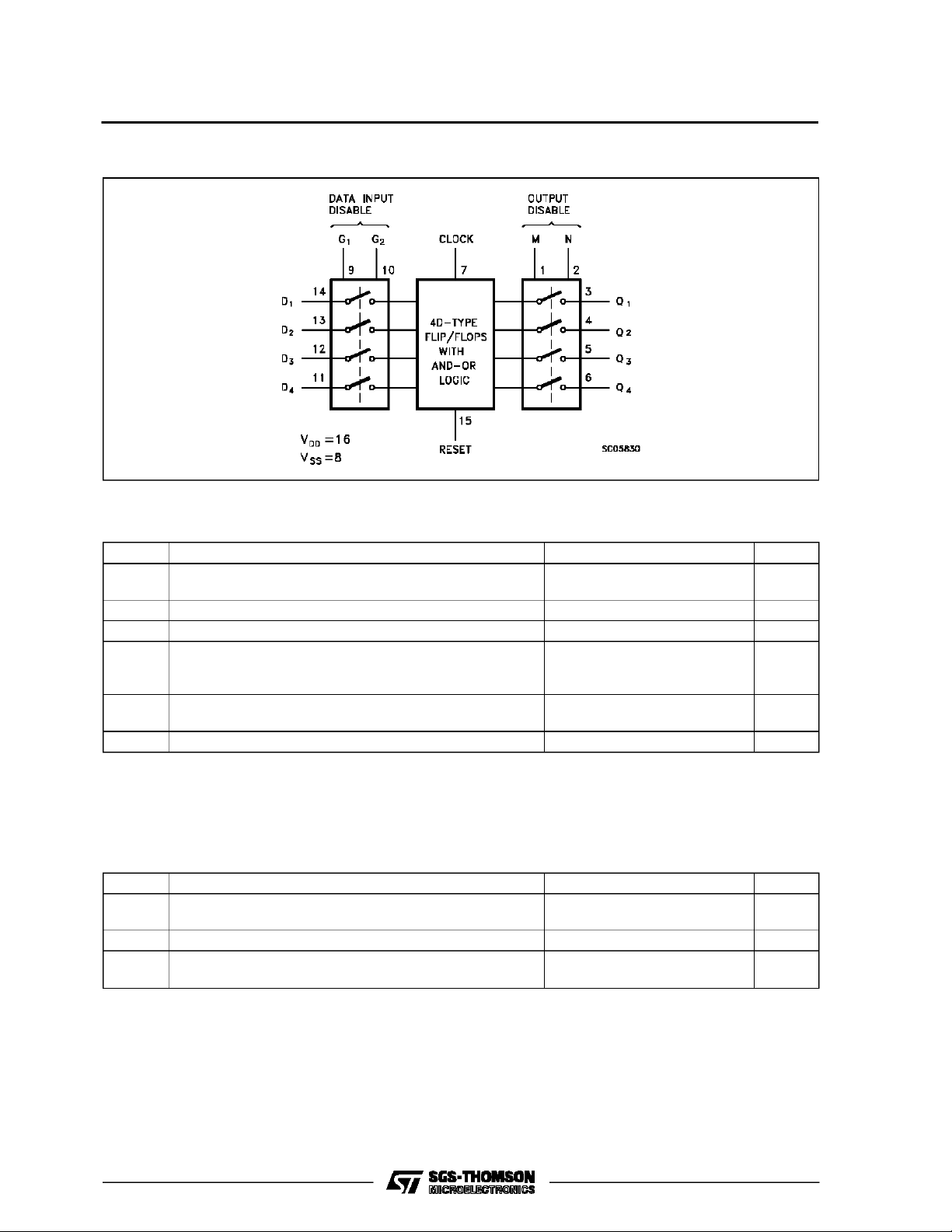
The HCC/HCF4076B types are four-bit registers
consisting of D-type flip-flops that feature threestate outputs. Data Disable inputs are provided to
controltheentryofdataintotheflip-flops.Whenboth
DataDisable inputsare low,data attheDinputsare
loaded into their respective flip-flops on the next
positivetransition of the click input. Output Disable
inputs are also provided. Whenthe OutputDisable
inputs are both low, the normal logic states of the
four outputs are available to the load. The outputs
are disabled independently of the clock by a high
logic level at either Output Disable input,and present a high impedance.
ORDER CODES :
HCC4 076BF HCF4076BM1
HCF4076BEY HCF4076BC1
PIN CONNECTIONS
September 1988
1/13
HCC/HCF4076B
FUN CTIONAL DIAG R A M
ABSOLU TE MAXIMU M RAT ING
Symbol Parameter Value Unit
V
* Supply Voltage: HCC Types
DD
HCF Types
V
P
Input Voltage -0.5 to VDD+ 0.5 V
i
I
DC Input Current (any one input) ± 10 mA
I
Total Power Dissipation (per package)
tot
Dissipation per Output Transistor
for Top = Full Package Temperature Range
T
Operating Temperature: HCC Types
op
HCF Types
T
Stressesabove those listedunder”AbsoluteMaximum Ratings”maycausepermanent damagetothedevice.Thisisastressratingonlyand functional
operation of the device at these or any otherconditions above thoseindicated in theoperational sections of thisspecificationisnotimplied.Exposure
to absolute maximum ratingconditionsforexternal periods mayaffect device reliability.
* All voltagevalues are referred to VSSpinvoltage.
Storage Temperature -65 to +150
stg
-0.5 to +20
-0.5 to +18
200
100
-55 to +125
-40 to +85
V
V
mW
mW
o
C
o
C
o
C
RECO MM ENDED OPERATING C O NDITIONS
Symbol Parameter Value Unit
V
V
T
2/13
Supply Voltage: HCC Types
DD
HCF Types
Input Voltage 0 to V
I
Operating Temperature: HCC Types
op
HCF Types
3to18
3to15
DD
-55 to +125
-40 to +85
V
V
V
o
C
o
C
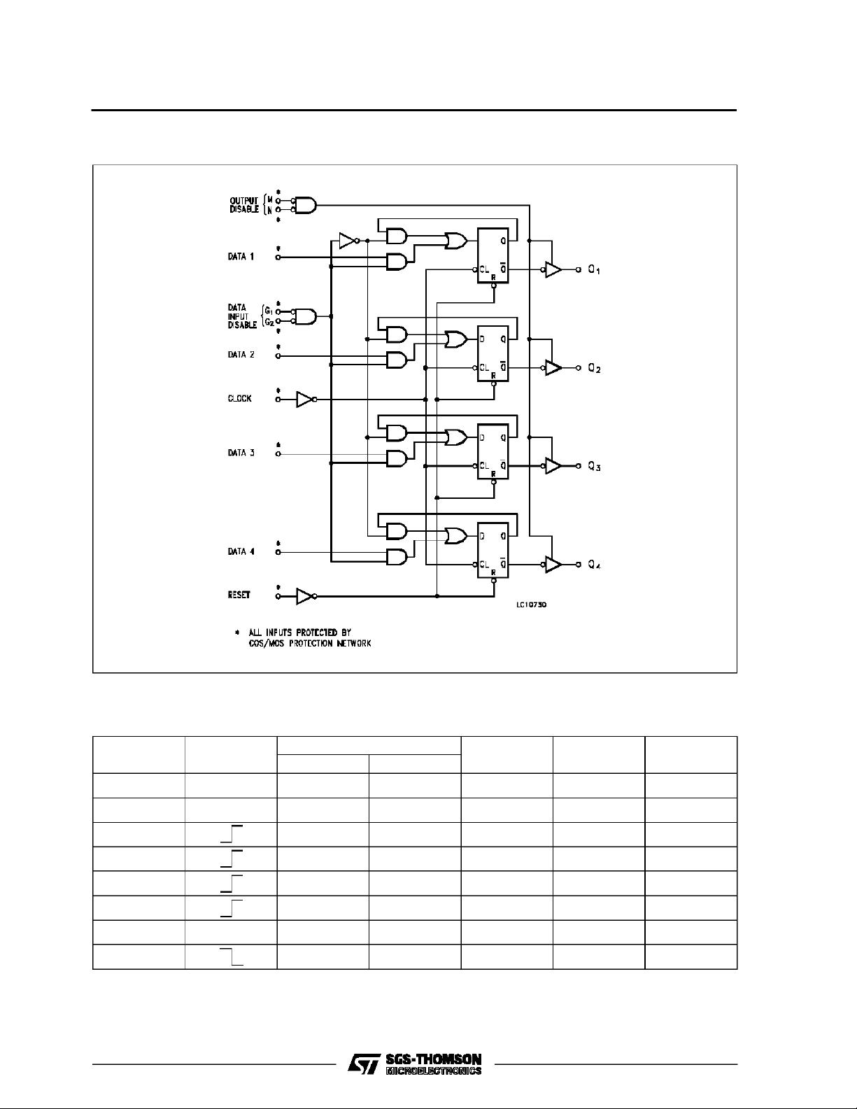
LOGI C DIAGRAM
HCC/HCF4076B
TRUTH TABLE
RESET CLOCK
1XXXX0
00XXXQNC
0 1XXQNC
0X1XQNC
00011
00000
01XXXQNC
0 XXXQNC
WheneitherOutputDisableMorNishigh, theoutputsaredisablesd(highimpedance state):howeversequential operation oftheflip-flopisnot affected.
1 = HighLevel, 0 = Low Level, X = Don’tCare, NC= No Change
DATA INPUT DISABLE DATA
G1 G2
D
NEXT STATE
OUTPUT G
3/13
HCC/HCF4076B
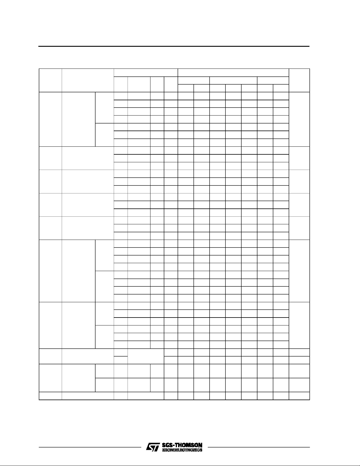
STATI C ELECT RIC AL CHAR ACTER I STI CS (ov er recomm end ed operating conditions)
Test Conditios Value
Symbol Parameter
Quiescent
I
L
Current
HCC
Types
V
(V)
V
I
(V)
|IO|
(µA)
V
(V)
O
T
DD
*25
LOW
Min. Max. Min. Typ. Max. Min. Max.
0/5 5 5 0.04 5 150
0/10 10 10 0.04 10 300
0/15 15 20 0.04 20 600
o
CT
0/20 20 100 0.08 100 3000
HCF
Types
0/5 5 20 0.04 20 150
0/10 10 40 0.04 40 300
0/15 15 80 0.04 80 600
OH
Output High
V
Voltage
0/5 < 1 5 4.95 4.95 4.95
0/10 < 1 10 9.95 9.95 9.95
0/15 < 1 15 14.95 14.95 14.95
OL
Output Low
V
Voltage
5/0 < 1 5 0.05 0.05 0.05
10/0 < 1 10 0.05 0.05 0.05
15/0 < 1 15 0.05 0.05 0.05
IH
Input High
V
Voltage
0.5/4.5 < 1 5 3.5 3.5 3.5
1/9 < 1 10 7 7 7
1.5/13.5 < 1 15 11 11 11
IL
Input Low
V
Voltage
4.5/0.5 < 1 5 1.5 1.5 1.5
9/1 < 1 10 3 3 3
13.5/1.5 < 1 15 4 4 4
OH
Output
Drive
Current
HCC
Types
I
0/5 2.5 5 -2 -1.6 -3.2 -1.15
0/5 4.6 5 -0.64 -0.51 -1 -0.36
0/10 9.5 10 -1.6 -1.3 -2.6 -0.9
0/15 13.5 15 -4.2 -3.4 -6.8 -2.4
0/5 2.5 5 -1.53 -1.36 -3.2 -1.1
HCF
Types
0/5 4.6 5 -0.52 -0.44 -1 -0.36
0/10 9.5 10 -1.3 -1.1 -2.6 -0.9
0/15 13.5 15 -3.6 -3.0 -6.8 -2.4
I
OL
Output
Sink
Current
HCC
Types
HCF
Types
0/5 0.4 5 0.64 0.51 1 0.36
0/10 0.5 10 1.6 1.3 2.6 0.9
0/15 1.5 15 4.2 3.4 6.8 2.4
0/5 0.4 5 0.61 0.44 1 0.36
0/10 0.5 10 1. 1.1 2.6 0.9
0/15 1.5 15 3.6 3.0 6.8 2.4
I
IH,IIL
Input Leakage
Current
I
OH,IOL
Input
Leakage
Current
HCC
Types
HCF
Types
C
*T
LOW
*T
HIGH
TheNoiseMargin for both”1” and”0” levelis: 1Vmin.withVDD=5V,2 V min.withVDD=10V,2.5 V min. withVDD=15V
Input Capacitance Any Input 5 7.5 pF
I
=-55oCforHCCdevice: -40oC for HCF device.
=+125oCforHCC device: +85oC for HCF device.
0/18
0/15 15 ±0.3 ±10
Any Input
18 ±0.1 ±10-5±0.1 ±1 µA
0/18 0/18 18 ±0.4 ±10
0/15 0/15 15 ±1.0 ±10
-5
±0.3 ±1 µA
-4
±0.4 ±12 µA
-4
±1.0 ±7.5 µA
HIGH
Unit
*
µA
V
V
V
V
mA
mA
4/13

HCC/HCF4076B
DYNAMIC ELECTRICAL CHARACTERISTICS (T
=25oC, CL=50pF,RL= 200 KΩ,
amb
typic al tem perat ur e coefficent for all VDDvalues is 03 %/oC, all input ris e and fall times= 20 ns )
Symbol Parameter
Propagation Delay Time
(Clock to Q Output)
(R) Propagation Delay Time
t
PHL
t
t
PLH
PHL
(Reset)
t
P(1-H)
t
P(0-H)
t
P(H-1)
t
P(L-1)
t
t
t
setup
t
setup
f
max
t
r,tf
3-State Output 1 or 0 to High Impedance RL=1KΩ 5 150 300
3-State High Impedance to 1 or 0 Output RL=1KΩ 5 150 300
Clock Pulse Width 5 200 100
W
Reset Pulse Width 5 120 60
W
Data Setup Time 5 200 100
Data Input Disable Setup Time 5 180 90
Maximum Clock Frequency 5 3 6
Clock Input Rise or Fall Time 5 15 µs
Test Conditions Value
(V) Min. Typ. Max.
V
DD
5 300 600
10 125 250
15 90 180
5 230 460
10 100 200
15 75 150
10 75 150
15 60 120
10 75 150
15 60 120
10 100 50
15 80 40
10 50 25
15 40 20
10 80 40
15 60 30
10 100 50
15 70 35
10 6 12
15 8 16
10 5
15 5
Unit
ns
ns
ns
ns
ns
ns
ns
ns
MHz
5/13

HCC/HCF4076B
Typical Output Low (sink) Current Characteristics
Typical Output High (source) Current Characteristics
Minimum Output Low (sink) Current Characteristics
Minimum Output High (source) Current Characteristics
Typical Maximum Clock Input Frequency vs Supply Voltage
6/13
Typical Dynamic Power Dissipation vs Frequency

HCC/HCF4076B
Typical Propagation Delay Time vs Capacitance
WAV EFORMS
Typical Transition Time vs Load Capacitance
7/13

HCC/HCF4076B
TEST CIRCUITS
QuiescentDevice Current. Noise Immunity.
Input Leakage Current.
8/13

Plastic DIP16 (0.25) MECHANICAL DATA
HCC/HCF4076B
DIM.
MIN. TYP. MAX. MIN. TYP. MAX.
a1 0.51 0.020
B 0.77 1.65 0.030 0.065
b 0.5 0.020
b1 0.25 0.010
D 20 0.787
E 8.5 0.335
e 2.54 0.100
e3 17.78 0.700
F 7.1 0.280
I 5.1 0.201
L 3.3 0.130
Z 1.27 0.050
mm inch
P001C
9/13

HCC/HCF4076B
Ceramic DIP16/1 MECHANICAL DATA
DIM.
MIN. TYP. MAX. MIN. TYP. MAX.
A 20 0.787
B 7 0.276
D 3.3 0.130
E 0.38 0.015
e3 17.78 0.700
F 2.29 2.79 0.090 0.110
G 0.4 0.55 0.016 0.022
H 1.17 1.52 0.046 0.060
L 0.22 0.31 0.009 0.012
M 0.51 1.27 0.020 0.050
N 10.3 0.406
P 7.8 8.05 0.307 0.317
Q 5.08 0.200
mm inch
10/13
P053D

SO16 (Narrow) MECHANICAL DATA
HCC/HCF4076B
DIM.
MIN. TYP. MAX. MIN. TYP. MAX.
A 1.75 0.068
a1 0.1 0.2 0.004 0.007
a2 1.65 0.064
b 0.35 0.46 0.013 0.018
b1 0.19 0.25 0.007 0.010
C 0.5 0.019
c1 45° (typ.)
D 9.8 10 0.385 0.393
E 5.8 6.2 0.228 0.244
e 1.27 0.050
e3 8.89 0.350
F 3.8 4.0 0.149 0.157
G 4.6 5.3 0.181 0.208
L 0.5 1.27 0.019 0.050
M 0.62 0.024
S8°(max.)
mm inch
P013H
11/13

HCC/HCF4076B
PLCC20 MECHANICAL DATA
DIM.
MIN. TYP. MAX. MIN. TYP. MAX.
A 9.78 10.03 0.385 0.395
B 8.89 9.04 0.350 0.356
D 4.2 4.57 0.165 0.180
d1 2.54 0.100
d2 0.56 0.022
E 7.37 8.38 0.290 0.330
e 1.27 0.050
e3 5.08 0.200
F 0.38 0.015
G 0.101 0.004
M 1.27 0.050
M1 1.14 0.045
mm inch
12/13
P027A

HCC/HCF4076B
Information furnished is believed to be accurate and reliable. However, SGS-THOMSON Microelectronics assumes no responsability forthe
consequences of use of such information nor for any infringement of patents or other rights of third parties which may results from its use. No
license is granted byimplicationor otherwise under any patentor patent rights ofSGS-THOMSON Microelectronics. Specificationsmentioned
in this publication aresubject to changewithout notice. This publication supersedes and replaces all information previously supplied.
SGS-THOMSON Microelectronicsproductsarenotauthorizedforuse ascriticalcomponentsinlifesupportdevicesorsystemswithoutexpress
written approval of SGS-THOMSON Microelectonics.
1994 SGS-THOMSON Microelectronics- All RightsReserved
Australia - Brazil - France - Germany - Hong Kong - Italy - Japan - Korea - Malaysia - Malta - Morocco - The Netherlands-
Singapore -Spain - Sweden - Switzerland - Taiwan - Thailand - UnitedKingdom - U.S.A
SGS-THOMSON Microelectronics GROUP OF COMPANIES
13/13
 Loading...