

ANALOG MULTIPLEXER/DEMULTIPLEXER
4067B–SINGLE 16-CHANNEL
4097B–DIFFERENTIAL 8-CHANNEL
.LOW ON RESISTANCE: 125Ω (typ.) OVER 15
Vp-p SIGNAL INPUTRANGE FOR
VDD-VSS= 15V
.HIGH OFF RESISTANCE: CHANNEL LEAK-
AGE OF ±10pA(typ.) @ VDD-VSS= 10V
.MATCHED SWITCH CHARACTERISTICS:
∆RON=5Ω(typ.) FORVDD-VSS= 15V
.VERY LOW QUIESCENT POWER DISSIPA-
TION UNDER A DIGITAL CONTROL INPUT
AND SUPPLY CONDITIONS: 0.2µW (typ.) @
VDD-VSS=10V
.BINARY ADDRESSDECODING ON CHIP
.QUIESCENT CURRENT SPECIFIED TO 20V
FOR HCC DEVICE
.STANDARDIZED SYMMETRICAL OUTPUT
CHARACTERISTICS
.5V, 10V AND 15VPARAMETRIC RATINGS
.INPUT CURRENTOF 100nAAT 18V AND25
FOR HCC DEVICE
o
C
.100% TESTED FOR QUIESCENTCURRENT
.MEETSALLREQUIREMENTSOFJEDECTEN-
TATIVE STANDARD No 13A, ”STANDARD
SPECIFICATIONS FOR DESCRIPTION OF B
SERIECMOS DEVICES”
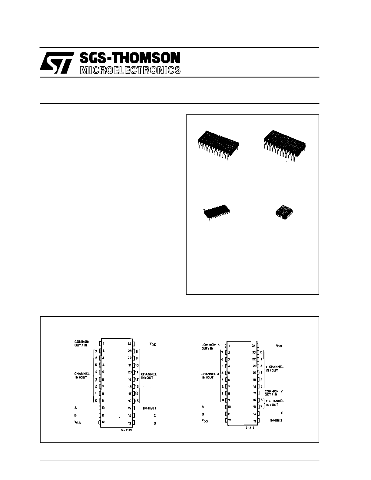
HCC/H CF 4 067 B
HCC/HCF4097B
EY
(PlasticPackage)
M1
(MicroPackage)
ORDER CODES :
HCC4 0XX BF HCF40XXBM 1
HCF40XXBEY HCF40XXBC1
(CeramicPackage)
(Chip Carrier)
F
C1
PIN CONNECTIONS
September 1988
4067B 4097B
1/16
HCC/H CF4067B HC C/ HCF4097B
DESCRIPTION
The HCC4067B, HCC4097B (extended temperaturerange) andHCF4067B,HCF4097B (intermedi-
ate temperature range) are monolithic integrated
circuitsavailable in24-lead dual in lineplastic or ceramic package.
The HCC/HCF4067B and HCC/HCF4097B
COS/MOS analog multiplexers/demultiplexers are
digitally controlled analog switches having low ON
impedance, low OFF leakage current and internal
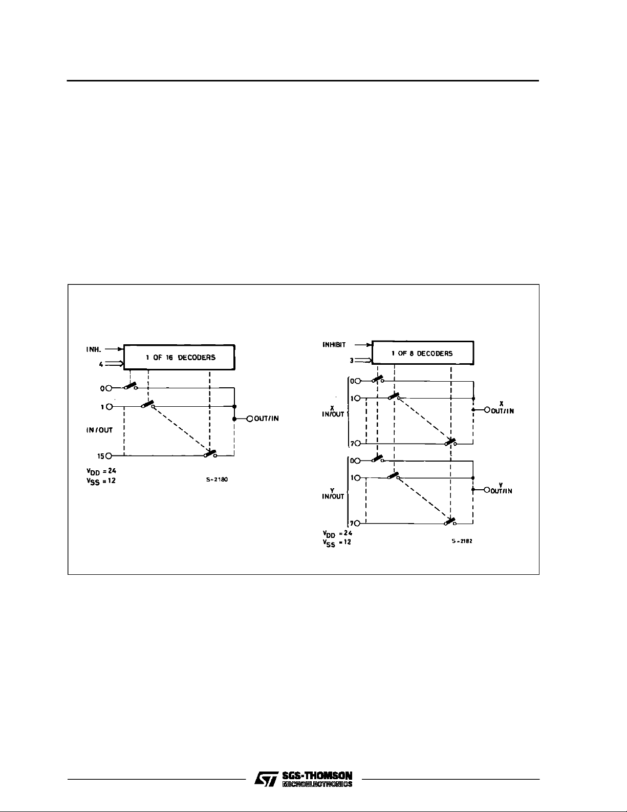
FUN CTIONAL DIAG R A M
For 4067B For 4097B
addressdecoding. in addition, the ON resistanceis
relatively constantover thefull input-signalrange.
The HCC/HCF4067B ia a 16-channel multiplexer
with fourbinary control inputs A, B, C, D, and an inhibit input,arranged so thatany combination of the
inputs selectsone switch.
TheHCC/HCF4097isa differential 8-channel multiplexerhaving threebinarycontrolinputsA,B,C,and
an inhibit input. The inputs permit selection of one
2/16
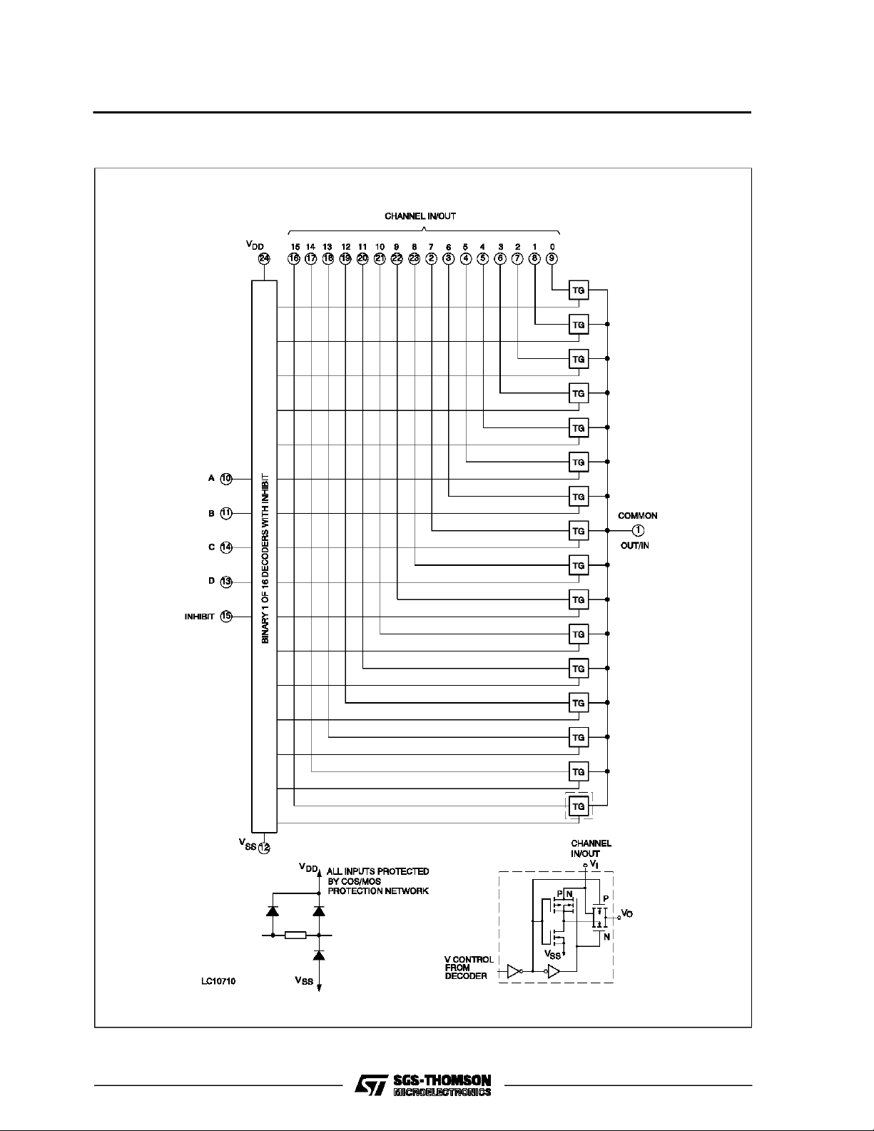
LOGI C DIAGRAM
HCC/HCF4067B HCC/HCF4097B
For 4067B
3/16
HCC/H CF4067B HC C/ HCF4097B
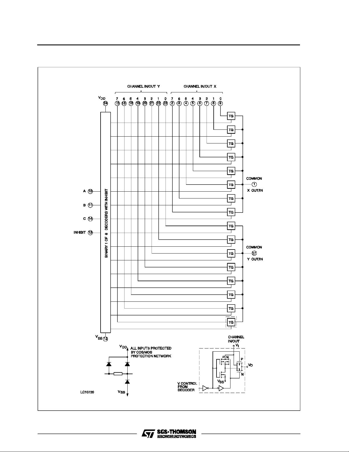
LOGI C DIAGRAM
For 4097B
4/16
HCC/HCF4067B HCC/HCF4097B
TRUTH TABLES FOR HCC/HCF4067B
A B C D INH
X X X X 1 None
00000 0
10000 1
01000 2
11000 3
00100 4
10100 5
01100 6
11100 7
00010 8
10010 9
01010 10
11010 11
00110 12
10110 13
01110 14
11110 15
SELECTED
CHANNEL
ABSOLU TE MAXI MUM R AT ING
TRUTH TABLE FOR HCC/HCF4097B
A B C INH
X X X 1 None
0000 0X0Y
1000 1X1Y
0100 2X2Y
1100 3X3Y
0010 4X4Y
1010 5X5Y
0110 6X6Y
1110 7X7Y
SELECTED
CHANNEL
Symbol Parameter Value Unit
V
* Supply Voltage: HCC Types
DD
HCF Types
V
P
Input Voltage -0.5 to VDD+ 0.5 V
i
I
DC Input Current (any one input) ± 10 mA
I
Total Power Dissipation (per package)
tot
-0.5 to +20
-0.5 to +18
200
V
V
mW
Dissipation per Output Transistor
for Top = Full Package Temperature Range
T
Operating Temperature: HCC Types
op
HCF Types
T
Stressesabove thoselistedunder ”AbsoluteMaximum Ratings”maycausepermanent damage to thedevice. Thisisa stressratingonlyand functional
operation of the device at these or any otherconditionsabove thoseindicated in theoperational sections of thisspecification isnotimplied.Exposure
to absolute maximum ratingconditions forexternal periods may affectdevice reliability.
* All voltagevalues arereferred to VSSpinvoltage.
Storage Temperature -65 to +150
stg
100
-55 to +125
-40 to +85
mW
o
C
o
C
o
C
RECO MM ENDED OPERATI N G CONDITI ONS
Symbol Parameter Value Unit
V
V
T
Supply Voltage: HCC Types
DD
HCF Types
Input Voltage 0 to V
I
Operating Temperature: HCC Types
op
HCF Types
3to18
3to15
DD
-55 to +125
-40 to +85
V
V
V
o
C
o
C
5/16

HCC/H CF4067B HC C/ HCF4097B
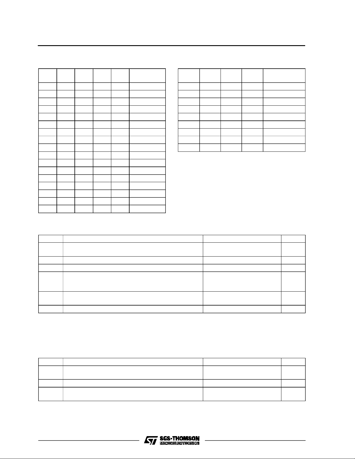
STATI C ELECT RIC AL CHA R ACTER IS TICS (over recommend ed operatin g c o ndi tions )
Symbol Parameter
Quiescent
I
L
Supply
Current
HCC
types
Test Conditios Value
V
V
V
(V)
IS
EE
(V)
(V)
SS
V
(V)
T
DD
*25
LOW
Min. Max. Min. Typ. Max. Min. Max.
5 5 0.04 5 150
10 10 0.04 10 300
15 20 0.04 20 600
o
CT
20 100 0.08 100 3000
HCF
types
5 20 0.04 20 150
10 40 0.04 40 300
15 80 0.04 80 600
SWITCH
ON
On
R
Resistance
∆ON Resistance ∆R
(Between any two
channels)
OFF(•)
Channel
Leakage
Current
Any
Channel OFF
All Channel
OFF
(common
HCC
types
HCF
types
ON
HCC
types
HCC
types
0 ≤ V
≤ V
0 ≤ V
≤ V
I
00
DD
I
00
DD
00
0 0 18 100 ±0.1 100 1000
0 0 18 100 ±0.1 100 1000
5 800 470 1050 1300
10 310 180 400 580
15 200 125 240 320
5 850 470 1050 1200
10 330 180 400 520
15 210 125 240 300
510
10 10
15 5
OUT/IN)
Any
Channel OFF
HCF
types
0 0 15 300 ±0.1 300 1000
All Channel
OFF
(common
HCF
types
0 0 15 300 ±0.1 300 1000
OUT/IN)
C Capacitance
Input
Output for 4067
Output for 4097
Feedthrough
-5 5
5
55
35
0.2
CONTROL
V
V
I
IHIIL
C
Input Low
IL
Voltage
Input High
IH
Voltage
Input
Leackage
Current
HCC
types
HCF
types
Input Capacitance Any Addressor
I
=V
thru
1KΩ
VEE=V
DD
RL=1KΩ
to V
SS
IIS<2µA
(onall OFF
channels)
V
= 0/18V 18 ±0.1 ±10-3±0.1 ±1
I
= 0/15V 15 ±0.3 ±10-3±0.3 ±1
V
I
5 1.5 1.5 1.5
SS
10 3 3 3
15 4 4 4
5 3.5 3.5 3.5
10 7 7 7
15 11 11 11
5 7.5
Inhibit Input
• Determined by minimum feasible leakagemeasurement forautomatic testing
*T
=-55oCforHCC device: -40oC for HCF device.
LOW
*T
=+125oCfor HCCdevice:+85oC for HCF device.
HIGH
TheNoiseMarginfor both ”1” and”0”level is: 1Vmin.withVDD=5V,2 V min.withVDD=10V,2.5 V min. withVDD=15V
HIGH
Unit
*
µA
Ω
Ω
µA
pF
V
V
µA
pF
6/16

HCC/HCF4067B HCC/HCF4097B
DYNAMIC ELECTRICAL CHARACTERISTICS (T
=25oC, CL=50pF,RL= 200 KΩ,
amb
typic al tem perature coeffic en t for all VDDvalues is 03 %/oC, all input rise and fall times = 20 ns)
Test Conditions Value
Symbol Parameter
SWITCH
Propagation Delay
t
pd
Time (Signal Input to
Output)
Frequency Response
Channel ”ON” (Sine
Wave Input) at
V
Log
V
O
I
=−3
dB
20
Feedthrough (All
Channels OFF) at
V
Log
O
V
=−40
I
20
Frequency Signal
Crosstalk at
V
O(B
20
Log
t
Sine Wave Distortion
W
)
=−40
V
I(A
)
(fis= 1KHz sine
wave)
CONTROL (address or Inhibit)
t
t
Propagation Delay
PLH
Time: Address or
PHL
Inhibit to Signal OUT
(Channel Turning ON)
dB
dB
V
(V)
R
f
V
V
C
(KΩ)
L
i
(KHz)
I
(V)
(V)
SS
V
(V)
DD
53060
=V
200 0
DD
10 15 30
15 11 20
=V
=V
15(•)0 10
DD
15(•)0 10
SS
at
V
O
Common
OUT/IN
at Any Channel 60
V
O
V
at
O
Common
OUT/IN
at Any Channel 8
V
O
4067B 14
4097B 20
4067B 20
4097B 12
Between Any two (A
and B) Channels
V
C(A)=VDD
V
C(B)=VSS
15(•)0 10
Between
Sections
(A and B)
4097B
only
Measured
on
common
Measured
on Any
Channel
51012(•) 0 5 0.3
10 10 1 3 (•) 0 10 0.2
15 10 1 5 (•) 0 15 0.12
0 5 325 650
1
0 10 135 270
0 15 95 190
Typ. Max.
1
10
18
Unit
ns
ns
MHz
MHz
ns
%
t
t
Propagation Delay
PLH
Time: Address or
PHL
Inhibit to Signal OUT
(Channel Turning
OFF)
Address or Inhibit to
Signal Crosstalk
(•)Peak to peakvoltage symmetrical about
(*)Both ends of channel
0 5 220 440
0 10 90 180
0.3
10* 0 10
V
−
V
DD
SS
2
0 15 65 130
75 mV
ns
peak
7/16

HCC/H CF4067B HC C/ HCF4097B
Typical ON Resistance vs Input Signal Voltage
(All Types)
Typical ON Resistance vs Input Signal Voltage
(All Types)
Typical ON Resistance vs Input Signal Voltage
(All Types)
Typical ON Resistance vs Input Signal Voltage
(All Types)
TEST CIRCUITS
OFF Channel Leakage Current Any Channel OFF
For 4067B For 4097B
8/16

HCC/HCF4067B HCC/HCF4097B
OFF Channel Leakage Current All Channels OFF
Input Voltage Measure < 2 µA an All OFF Channels (e.g. Channel 12)
For 4067B For 4097B
For 4097BFor 4067B
Quiescent Device Current
For 4067B For 4097B
9/16

HCC/H CF4067B HC C/ HCF4097B
Turn-on and Turn-off Propagation Delay Address Select Input to Signal Output (e. g. Channel 0)
For 4097BFor 4067B
Turn-on and Turn-off Propagation Delay-Inhibit Input to Signal Output (e. g. Channel 1)
For 4067B For 4097B
Channel ON Resistance Measurement Circuit
10/16

HCC/HCF4067B HCC/HCF4097B
Propagation Delay Waveform Channel Being
Turned ON (RL=10KΩ,CL= 50 pF)
APPLICATIONS INFORMATION
In applications where separate power sources are
usedtodriveVDDand thesignal inputs, theVDDcurrentcapability should exceedVDD/RL(RL= effective
externalload).Thisprovisionavoids permanent current flow or clamp action on the VDDsupply when
power is applied or removed from the
HCC/HCF4067Bor HCC/HCF4097B.
Whenswitchingfromone address toanother, some
oftheON periodsof thechannels ofthemultiplexers
will overlap momentarily, which may be objectionable in certainapplications. Also when a channel is
turned ON or OFF by an address input, there is a
momentary conductive path from the channel to
VSS,which willdrumpsomechargefromanycapacitorconnected tothe inputor output ofthe channel.
The inhibit input turning on a channel will similarly
drumpsome charge to VSS.
The amount of charge dumped is mostlya function
of the signal level above VSS.
Typically, ay VDD-VSS= 10V, a 100 pF capacitor
connected to the input or output of the channelwill
Propagation Delay Waveform Channel Being
Turned OFF (RL= 300 Ω,CL= 50 pF)
lose 3-4%of itsvoltage at the moment the channel
turns ON or OFF. This loss of voltage is essentially
independent of the address or inhibit signal trnasition time, if the transition time is less than 1- 2 µs.
When the inhibit signal turns a channel off, there is
no changedumping of VSS. Rather, there is a slight
risein the channel voltage level (65 mV typ.)due to
the capacitance coupling from inhibit inputto channel input or output. Address inputalso couplesome
voltagesteps onto the channelsignallevels.
In certain applications, the external load-resistor
current may include both VDDand signal line components.To avoiddrawing VDDcurrentwhen switch
current flows into the transmission gate inputs, the
voltagedrop acrossthebidirectionalswitchmustnot
exceed0.8 V (calculated fromRONvaluesshownin
ELECTRICAL CHARACTERISTICS CHART). No
VDDcurrent willflowthroughRLiftheswitchcurrent
flowsintoterminal1 on theHCC/HCF4067B, termi-
nals 1 and 17 on the HCC/HCF4097B.
11/16

HCC/H CF4067B HC C/ HCF4097B
Plastic DIP24 (0.25) MECHANICAL DATA
DIM.
MIN. TYP. MAX. MIN. TYP. MAX.
a1 0.63 0.025
b 0.45 0.018
b1 0.23 0.31 0.009 0.012
b2 1.27 0.050
D 32.2 1.268
E 15.2 16.68 0.598 0.657
e 2.54 0.100
e3 27.94 1.100
F 14.1 0.555
I 4.445 0.175
L 3.3 0.130
mm inch
12/16
P043A

HCC/HCF4067B HCC/HCF4097B
Ceramic DIP24 MECHANICAL DATA
DIM.
MIN. TYP. MAX. MIN. TYP. MAX.
A 32.3 1.272
B 13.05 13.36 0.514 0.526
C 3.9 5.08 0.154 0.200
D 3 0.118
E 0.5 1.78 0.020 0.070
e3 27.94 1.100
F 2.29 2.79 0.090 0.110
G 0.4 0.55 0.016 0.022
I 1.17 1.52 0.046 0.060
L 0.22 0.31 0.009 0.012
M 1.52 2.49 0.060 0.098
N1
P 15.4 15.8 0.606 0.622
Q 5.71 0.225
4° (min.), 15° (max.)
mm inch
P058C
13/16

HCC/H CF4067B HC C/ HCF4097B
SO24 MECHANICAL DATA
DIM.
MIN. TYP. MAX. MIN. TYP. MAX.
A 2.65 0.104
a1 0.10 0.20 0.004 0.007
a2 2.45 0.096
b 0.35 0.49 0.013 0.019
b1 0.23 0.32 0.009 0.012
C 0.50 0.020
c1 45° (typ.)
D 15.20 15.60 0.598 0.614
E 10.00 10.65 0.393 0.420
e 1.27 0.05
e3 13.97 0.55
F 7.40 7.60 0.291 0.299
L 0.50 1.27 0.19 0.050
S8°(max.)
mm inch
L
A
a2
b
e3
D
24 13
112
e
F
s
a1
c1
b1
C
E
14/16

HCC/HCF4067B HCC/HCF4097B
PLCC20 MECHANICAL DATA
DIM.
MIN. TYP. MAX. MIN. TYP. MAX.
A 9.78 10.03 0.385 0.395
B 8.89 9.04 0.350 0.356
D 4.2 4.57 0.165 0.180
d1 2.54 0.100
d2 0.56 0.022
E 7.37 8.38 0.290 0.330
e 1.27 0.050
e3 5.08 0.200
F 0.38 0.015
G 0.101 0.004
M 1.27 0.050
M1 1.14 0.045
mm inch
P027A
15/16

HCC/H CF4067B HC C/ HCF4097B
Information furnished is believed tobe accurate and reliable. However, SGS-THOMSON Microelectronics assumes no responsability for the
consequences of use of such information nor for any infringement of patents or other rights of third parties which may results from its use. No
license is granted byimplicationor otherwise under any patentor patent rights ofSGS-THOMSONMicroelectronics. Specificationsmentioned
in this publication are subject to change without notice. Thispublication supersedes and replaces all information previously supplied.
SGS-THOMSON Microelectronicsproductsarenotauthorizedforuse ascriticalcomponentsinlifesupportdevicesorsystemswithoutexpress
written approval of SGS-THOMSON Microelectonics.
1994 SGS-THOMSON Microelectronics- All Rights Reserved
Australia - Brazil - France - Germany - HongKong - Italy - Japan - Korea - Malaysia - Malta - Morocco - The Netherlands -
Singapore -Spain - Sweden - Switzerland -Taiwan - Thailand - UnitedKingdom - U.S.A
SGS-THOMSON Microelectronics GROUP OF COMPANIES
16/16
 Loading...