

Datasheet HCF4066BM1, HCF4066BEY, HCF4066BC1, HCC4066BF Datasheet (SGS Thomson Microelectronics)
QUAD BILATERAL SWITCHFOR TRANSMISSION
OR MULTIPLEXINGOF ANALOG ORDIGITAL SIGNALS
.15V DIGITAL OR ± 7.5V PEAK-TO-PEAK
SWITCHING
.80Ω TYPICAL ON RESISTANCE FOR 15V
OPERATION
.SWITCH ON RESISTANCE MATCHED TO
WITHIN 5Ω OVER 15V SIGNAL-INPUT
RANGE
.ON RESISTANCE FLAT OVER FULL PEAK-
TO-PEAKSIGNALRANGE
.HIGH ON/OFFOUTPUT-VOLTAGE RATIO:
65dB TYP.@ fis= 10kHz,RL= 10kΩ
.HIGH DEGREE OF LINEARITY : < 0.5% DIS-
TORTIONTYP. @ fis= 1kHz, Vis= 5 Vp-p,
VDD–VSS≥ 10V,RL=10kΩ
.EXTREMELY LOW OFF SWITCH LEAKAGE
RESULTING IN VERY LOW OFFSET CURRENT AND HIGH EFFECTIVE OFF RESISTANCE; 10pA TYP. @ VDD–VSS= 10V,
TA=25°C
.EXTREMELY HIGH CONTROL INPUTIMPED-
ANCE (control circuit isolated from signal circuit): 1012Ω TYP.
.LOW CROSSTALK BETWEEN SWITCHES:–
50dB TYP.@ fis= 0.9MHz,RL=1kΩ
.MATCHED CONTROL-INPUT TO SIGNAL-
OUTPUT CAPACITANCE : REDUCES OUTPUT SIGNALTRANSIENTS
.FREQUENCYRESPONSE,SWITCH ON =
40MHz (typ.)
.QUIESCENT CURRENT SPECIFIED TO 20V
FOR HCC DEVICE
.5V, 10V, AND 15V PARAMETRIC RATINGS
.INPUT CURRENT OF 100nAAT 18V AND 25°C
FOR HCC DEVICE
.100% TESTEDFOR QUIESCENTCURRENT
.MEETSALLREQUIREMENTSOFJEDECTEN-
TATIVE STANDARD No. 13A, ”STANDARD
SPECIFICATIONS FOR DESCRIPTION OF ”B”
SERIESCMOS DEVICES”
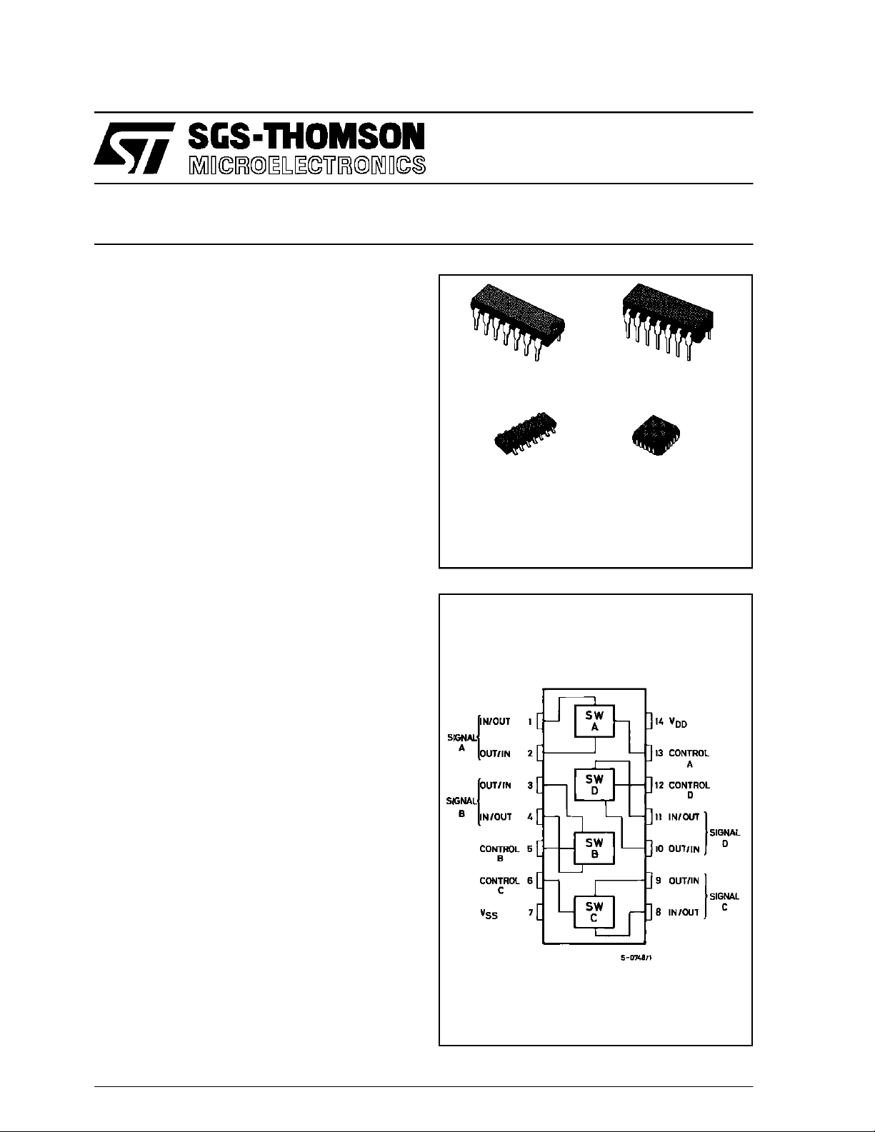
HCC/HCF4066B
EY
(Plastic Package)F(Ceramic FritSeal Package)
M1
(MicroPackage)
ORDER CODES :
HCC4066BF HCF4066BM1
HCF4066BEY HCF4066BC1
PIN CONNECTIONS
(PlasticChipCarrier)
C1
DESCRIPTI ON
TheHCC4066B (extended temperature range) and
HCF4066B (intermediate temperature range) are
monolithic integrated circuits, available in 14-lead
dual in-line plastic or ceramic package and plastic micropackage. The HCC/HCF4066B is a quad
bilateral switch intended for the transmission or
multiplexing of analog or digital signals. It is pin-for-
June1989
1/11
HCC/HCF4066B
pin compatiblewithHCC/HCF4016B, butexhibits a
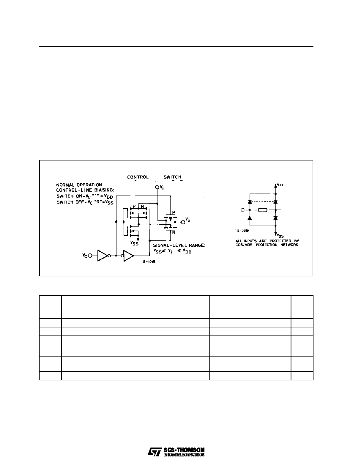
much lower ON resistance. In addition, the ON resistanceis relativelyconstantoverthe full input-signal range. The HCC/HCF4066B consists of four
independent bilateralswitches.Asinglecontrol signal is required per switch.Both the p and the n device in a given switch are biased ON or OFF
simultaneously by the control signal. As shown in
schematicdiagram, the wellof then-channel device
configuration eliminates the variation of theswitchtransistor threshold voltage with input signal, and
thus keepsthe ON resistance low over the fulloperating-signal range. The advantages over singlechannel switches include peak input signal voltage
swings equal to the full supply voltage, and more
constant ON impedance over the input-signal
range. For sample-and-hold applications, however,
the HCC/HCF4016B is recommended.
on each switch is either tied to the input when the
switchis ON or to VSSwhentheswitchis OFF.This
SCHEM ATIC D IA GRAM
1 OF 4 IDENTICALSWITCHES AND ITS ASSOCIATED CONTROL CIRCUITRY.
ABSOLUTE M AXIMUM RAT IN G S
Symbol Parameter Value Unit
* Supply Voltage :HC C Types
V
DD
V
Input Voltage – 0.5 to VDD+ 0.5 V
i
DC Input Current (any one input) ± 10 mA
I
I
P
T
T
Stresses above those listed under ”Absolute Maximum Ratings” may cause permanent damage to the device. This is a stress
rating only and functional operation of the device at these or any other conditions above those indicated in the operational sections
of this specification is not implied. Exposure to absolute maximum rating conditions for external periods may affect device reliability.
* All voltage values are referred to VSSpin voltage.
2/11
Total Power Dissipation ( per package)
tot
Dissipation per Output Transistor
for T
Operating Temperature : HCC Types
op
Storage Temperature – 65 to + 150 °C
stg
= Full Package-temperature Range
op
HCF Types
HCF Types
– 0.5 to + 20
– 0.5 to + 18
200
100
– 55 t o + 125
–40to+85
V
V
mW
mW
°C
°C
HCC/HCF4066B
RECOMMENDED OPERATING CONDITIONS
Symbol Parameter Value Unit
V
T
ELECTRICAL CHARACTERISTICS
(T
amb
Symbol Parameter
SIGNAL I N PU T S (V
R
∆ON Resistance
TDH Total Harmonic
*T
Low
*T
High
The Noise Margin for both ”1” and ”0” level is : 1V min. with VDD= 5V, 2V min. with VDD= 10V, 2.5V min. with VDD= 15V.
Supply Voltage :HC C Types
DD
HCF Types
V
Input Voltage 0 to V
I
Operating Temperature : HCC Types
op
HCF Types
=25°C,typical temperature coefficient forall VDDvalues is 0,3%/°C)
Test Conditions Value
T
* 25°CT
Low
Min. Max. Min. Typ. Max. Min. Max.
I
L
Quiescent
Device
Current (all
switches
ON or all
switches
OFF)
HCC
Types
HCF
Types
0/ 5 5 0.25 0.01 0.25 7.5
0/10 10 0.5 0.01 0.5 15
0/15 15 1 0.01 1 30
0/20 20 5 0.02 5 150
0/ 5 5 1 0.01 1 7.5
0/10 10 2 0.01 2 15
0/15 15 4 0.01 4 30
) and Outputs (Vos)
is
ON
On
Resistance
HCC
Types
HCF
V
C=VDD
RL= 10KΩ Return
V
________
DD–VSS
to
2
V
is=VSS
to V
DD
Types
RL10kΩ,VC=VDD515
between any 2
Switches, ∆R
Distorsion
- 3 dB Cutof f
Frequency(switch
on)
ON
V
C=VDD
V
SS
V
is
(sinewave centeredin 0V)
R
L
f
is
V
C=VDD
V
SS
V
is
(sine wave c entured on
= 5V,
= – 5V,
(p-p) = 5V
= 10k Ω,
= 1kHz s ine wav e
=5V,
=–5V,
(p-p) = 5V
0V)
=1kΩ
R
L
=–55°CforHCC device : – 40°CforHCF device.
= + 125°CforHCC device : + 85°CforHCF device.
V
IVDD
(V) (V)
5 800 470 1050 1300
10 310 180 400 550
15 200 125 240 320
5 850 470 1050 1200
10 330 180 400 500
15 210 125 240 300
10 10
15 5
3to18
3to15
– 55 t o + 125
–40to+85
0.4
40
DD
High
°C
°C
*
Unit
µA
Ω
Ω
%
MHz
V
V
V
3/11
HCC/HCF4066B
ELECTRICAL CHARACTERISTICS(continued)
Test Conditions Va lu e
Symbol Parameter
V
(V)
-50dB
Feedthrough
Frequency(switch
off)
- 50 dB Crosstalk
Frequency
V
C=VSS
V
is
(sine wave centured on
0V)
R
L
V
C
VC(B) = VSS=–5V
V
is
=–5V,
(p-p) = 5V
=1kΩ
(A) = VDD=+5V
(A) = 5Vp-p,
50Ω source
R
=1kΩ
L
PropagationDelay
t
pd
(signal input to
signaloutput)
RL= 200kΩ
VC=VDD,VSS= GND,
C
= 50pF , Vis=10V
L
(square wave centured on
5V)
t
= 20ns
r,tf
C
Input Capacitance VDD=+5V
is
Output
C
os
VC=VSS=–5V
Capacitance
C
CONTROL (V
V
V
Feedthrough 0.5
ios
Input/Output
Leakage
Current
Switch OFF
Control Input Low
ILC
Voltage
Control Input High
IHC
Voltage
)
C
V
HCC
Types
HCF
Types
C
V
is
=0V
V
is
=18V
V
C
V
is
=0V
V
is
=15V
Iis <10µA
Vis=VSS,Vos=V
and
Vis=VDD,Vos=V
=0V
= 18V ; V
=0V;V
=0V
= 15V ; V
=0V;V
os
os
os
os
18
15 ± 0.3 ±10
DD
10 2 2 2
15 2 2 2
SS
10 7 7 7
15 11 11 11
I
IH,IIL
*T
=–55°CforHCC device : – 40°CforHCF device.
Low
*T
= + 125°CforHCC device : + 85°CforHCF device.
High
The Noise Margin for both ”1” and ”0” level is : 1V min. with VDD= 5V, 2V min. with VDD= 10V, 2.5V min. with VDD= 15V.
Input
Leakage
Current
HCC
Vis≤ V
Types
VDD–VSS= 18V
HCF
V
VCC≤ VDD–V
Types
DD
DD–VSS
= 15V
SS
18 ± 0.1 ±10
15 ± 0.3 ±10–5± 0.3 ± 1
T
DD
* 25°CT
Low
* Unit
High
Min. Max. Min. Typ. Max. Min. Max.
1MHz
8MHz
52040
10 10 20
ns
15 7 15
8
pF
± 0.1 ±10
8
–3
± 0.1 ± 1
µA
–3
± 0.3 ± 1
51 11
V
5 3.5 3.5 3.5
V
–5
± 0.1 ± 1
µA
4/11

HCC/HCF4066B
ELECTRICAL CHARACTERISTICS (continued)
Test Condi t io n s Va lue
Symbol Parameter
V
DD
(V)
Crosstalk(control
input to signal
output)
Turn-on
Propagation Delay
Control Input
Repetition Rate
= 10V (sq. wave)
V
C
tr,tf=20ns
R
=10kΩ
L
V
IN=VDD
tr,tf=20ns
CL=50pF
R
=1kΩ
L
V
is=VDD,VSS
R
=1kΩto gnd
L
10 50 mV
53570
10 20 40
15 15 30
= GND
56
CL=50pF
V
= 10V (square
C
wave c entured on
10 9
5V)
t
=20ns
r,tf
Vos=1/2Vos@1kHz
C
Input Capacitance Any Input 5 7.5 pF
I
*T
=–55°CforHCC device : – 40°CforHCF device.
Low
*T
= + 125°CforHCC device : + 85°CforHCF device.
High
The Noise Margin for both ”1” and ”0” level is : 1V min. with VDD= 5V, 2V min. with VDD= 10V, 2.5V min. with VDD= 15V.
15 9.5
T
* 25 °CT
Low
* Unit
High
Min. Max. Min. Typ. Max. Min. Max.
ns
MHz
TYPICAL APPLI CA TI O NS
BIDIRECTIONALSIGNAL TRANSMISSION VIA DIGITAL CONTROL LOGIC
5/11

HCC/HCF4066B
TYPICAL APPLI CA TI O NS (continued )
4-CHANNEL PAM MULTIPLEX SYSTEMDIAGRAM.
6/11

Plastic DIP14 MECHANICAL DATA
HCC/HCF4066B
DIM.
MIN. TYP. MAX. MIN. TYP. MAX.
a1 0.51 0.020
B 1.39 1.65 0.055 0.065
b 0.5 0.020
b1 0.25 0.010
D 20 0.787
E 8.5 0.335
e 2.54 0.100
e3 15.24 0.600
F 7.1 0.280
I 5.1 0.201
L 3.3 0.130
Z 1.27 2.54 0.050 0.100
mm inch
P001A
7/11

HCC/HCF4066B
Ceramic DIP14/1 MECHANICAL DATA
DIM.
MIN. TYP. MAX. MIN. TYP. MAX.
A 20 0.787
B 7.0 0.276
D 3.3 0.130
E 0.38 0.015
e3 15.24 0.600
F 2.29 2.79 0.090 0.110
G 0.4 0.55 0.016 0.022
H 1.17 1.52 0.046 0.060
L 0.22 0.31 0.009 0.012
M 1.52 2.54 0.060 0.100
N 10.3 0.406
P 7.8 8.05 0.307 0.317
Q 5.08 0.200
mm inch
8/11
P053C

SO14 MECHANICAL DATA
HCC/HCF4066B
DIM.
MIN. TYP. MAX. MIN. TYP. MAX.
A 1.75 0.068
a1 0.1 0.2 0.003 0.007
a2 1.65 0.064
b 0.35 0.46 0.013 0.018
b1 0.19 0.25 0.007 0.010
C 0.5 0.019
c1 45° (typ.)
D 8.55 8.75 0.336 0.344
E 5.8 6.2 0.228 0.244
e 1.27 0.050
e3 7.62 0.300
F 3.8 4.0 0.149 0.157
G 4.6 5.3 0.181 0.208
L 0.5 1.27 0.019 0.050
M 0.68 0.026
S8°(max.)
mm inch
P013G
9/11

HCC/HCF4066B
PLCC20 MECHANICAL DATA
DIM.
MIN. TYP. MAX. MIN. TYP. MAX.
A 9.78 10.03 0.385 0.395
B 8.89 9.04 0.350 0.356
D 4.2 4.57 0.165 0.180
d1 2.54 0.100
d2 0.56 0.022
E 7.37 8.38 0.290 0.330
e 1.27 0.050
e3 5.08 0.200
F 0.38 0.015
G 0.101 0.004
M 1.27 0.050
M1 1.14 0.045
mm inch
10/11
P027A

HCC/HCF4066B
Information furnished is believed tobe accurate and reliable. However, SGS-THOMSON Microelectronics assumes no responsability for the
consequences of use of such information nor for any infringement of patents or other rights of third parties which may results from its use. No
license is granted by implication or otherwise underany patent or patent rights of SGS-THOMSON Microelectronics. Specificationsmentioned
in this publicationare subject to changewithout notice. This publication supersedes and replaces all information previously supplied.
SGS-THOMSON Microelectronicsproductsare notauthorized for use ascritical componentsinlife supportdevices or systemswithout express
written approval of SGS-THOMSON Microelectonics.
1994 SGS-THOMSON Microelectronics- All Rights Reserved
Australia - Brazil - France - Germany - Hong Kong - Italy - Japan - Korea - Malaysia - Malta - Morocco - The Netherlands -
Singapore - Spain - Sweden - Switzerland - Taiwan - Thailand - United Kingdom - U.S.A
SGS-THOMSON Microelectronics GROUP OF COMPANIES
11/11
 Loading...