


ANALOG MULTIPLEXERS-DEMULTIPLEXERS
4051B - SINGLE 8-CHANNEL
405 2B - DIFFER ENTIAL 4- CHA N NEL
4053B - TRIPLE 2-CHANNEL
.QUIESCENT CURRENT SPECIFIED TO 20V
FOR HCC DEVICE
.LOW ”ON” RESISTANCE : 125Ω (typ.) OVER
15V p.p. SIGNAL-INPUT RANGE FOR VDDVEE=15V
.HIGH ”OFF” RESISTANCE: CHANNEL LEAK-
AGE ± 100pA (typ.) VDD–VEE= 18V
.BINARYADDRESSDECODINGON CHIP
.VERY LOW QUIESCENT POWER DISSIPA-
TION UNDERALL DIGITAL CONTROLINPUT
AND SUPPLY CONDITIONS : 0.2 µW (typ.),
VDD–VSS=VDD–VEE=10V
.MATCHED SWITCH CHARACTERISTICS :
RON=5Ω (typ.)for VDD–VEE=15V
.WIDE RANGEOF DIGITALANDANALOGSIG-
NAL LEVELS :DIGITAL3TO20V,ANALOG TO
20V p.p.
.5V, 10V,AND 15VPARAMETRIC RATINGS
.INPUT CURRENT OF 100mA AT 18V AND
25°C FORHCC DEVICE
.100% TESTEDFOR QUIESCENTCURRENT
.MEETSALLREQUIREMENTSOFJEDECTEN-
TATIVE STANDARD No13A, ”STANDARD
SPECIFICATIONS FOR DESCRIPTION OF”B”
SERIESCMOS DEVICES”
HCC4051B/52B/53B
HCF4051B/52B/53B
EY
(Plastic Package)F(CeramicFritSeal Package)
M1
(MicroPackage)C1(Plastic Chip Carrier)
ORDERCODES :
HCC40XXBF HCF40XXBM1
HCF40XXBEY HCF40XXBC1
DESCRIPTION
TheHCC 4051B,4052B and4053B(extendedtem-
peraturerange)andHCF4051B,4052Band4053B
(intermediate temperature range) aremonolithic integrated circuits, available in 16-lead dual in-line
plastic or ceramic package and plastic micropackage. HCC/HCF4051B, HCC/HCF4052B, and
HCC/HCF4053B analog multiplexers/demulti-
plexersaredigitally controlled analog switcheshaving low ON impedance and very low OFF leakage
PIN CONNECTIONS
4051B
June 1989
4052B 4053B
1/17

HCC/H CF4051B/52B/53B
current. These multiplexer circuits dissipate extremelylowquiescent powerover the full VDD–V
SS
and VDD–VEEsupply-voltageranges, independent
ofthelogic state ofthecontrol signals. Whena-logic
”1” ispresent at the inhibit inputterminalall channel
are off. The HCC/HCF4051B is a single8-channel
multiplexer having threebinarycontrolinputs, A,B,
and C, and an inhibit input.The three binary signals
select1 of8 channels to be turned on,and connect
one of the 8 inputs to the output. The
HCC/HCF4052B is a differential 4-channel multi-
FUNCTIONAL DIAGRAMS AND TRUTH TABLES
4051B
plexerhaving twobinarycontrolinputs, AandB,and
an inhibitinput. The two binaryinput signals select
1 of 4pairs of channels tobe turned on and connect
the analog inputs to the outputs. The
HCC/HCF4053B is a triple 2-channel multiplexer
having three separate digital control inputs, A, B,
and C, and an inhibit input. Each control input selects one of a pair of channels whichare connected
in asinglepoledouble-throw configuration.
Input States
Inhibit C B A
0000 0
0001 1
0010 2
0011 3
0100 4
0101 5
0110 6
0111 7
1 X X X None
”On” Channel (S)
2/17
4052B
Inhibit B A
0 0 0 0x, 0y
0 0 1 1x, 1y
0 1 0 2x, 2y
0 1 1 3x, 3y
1 X X None

FUNCTIONAL DIAGRAMS AND TRUTH TABLES (continued)
HCC/HCF4051B/52B/53B
4053
Inhibit
0 0 ax or bx or cx
0 1 ay or by or cy
1 X None
X = Don’t care.
AorB
or C
ABSOLUTE M AXI MUM RAT IN GS
Symbol Parameter Value Unit
V
* Supply Voltage : HCC Types
DD
HCF Types
V
Input Voltage – 0.5 to VDD+ 0.5 V
i
I
DC Input Current (any one input) ± 10 mA
I
P
Total Power Dissipation (per package)
tot
– 0.5 to + 20
– 0.5 to + 18
200
V
V
mW
Dissipation per Output Transistor
for T
T
T
Stresses above those listed under ”Absolute Maximum Ratings” may cause permanent damage to the device. This is a stress
rating only and functional operation of the device at these or any other conditions above those indicated in the operational sections of this specification is not implied. Exposure to absolute maximum rating conditions for external periods may affect device
reliability.
* All voltage values are referred to VSSpin voltage.
Operating Temperature : HCC Types
op
Storage Temperature – 65 to + 150 °C
stg
= Full Package-temperature Range
op
HCF Types
100
– 55 to + 125
–40to+85
mW
°C
°C
RECOMMENDED OPERATING CONDITIONS
Symbol Parameter Value Unit
V
T
Supply Voltage :HCC Types
DD
HCF Types
V
Input Voltage 0 to V
I
Operating Temperature : HCC Types
op
HCF Types
3to18
3to15
DD
– 55 to + 125
–40to+85
V
V
V
°C
°C
3/17
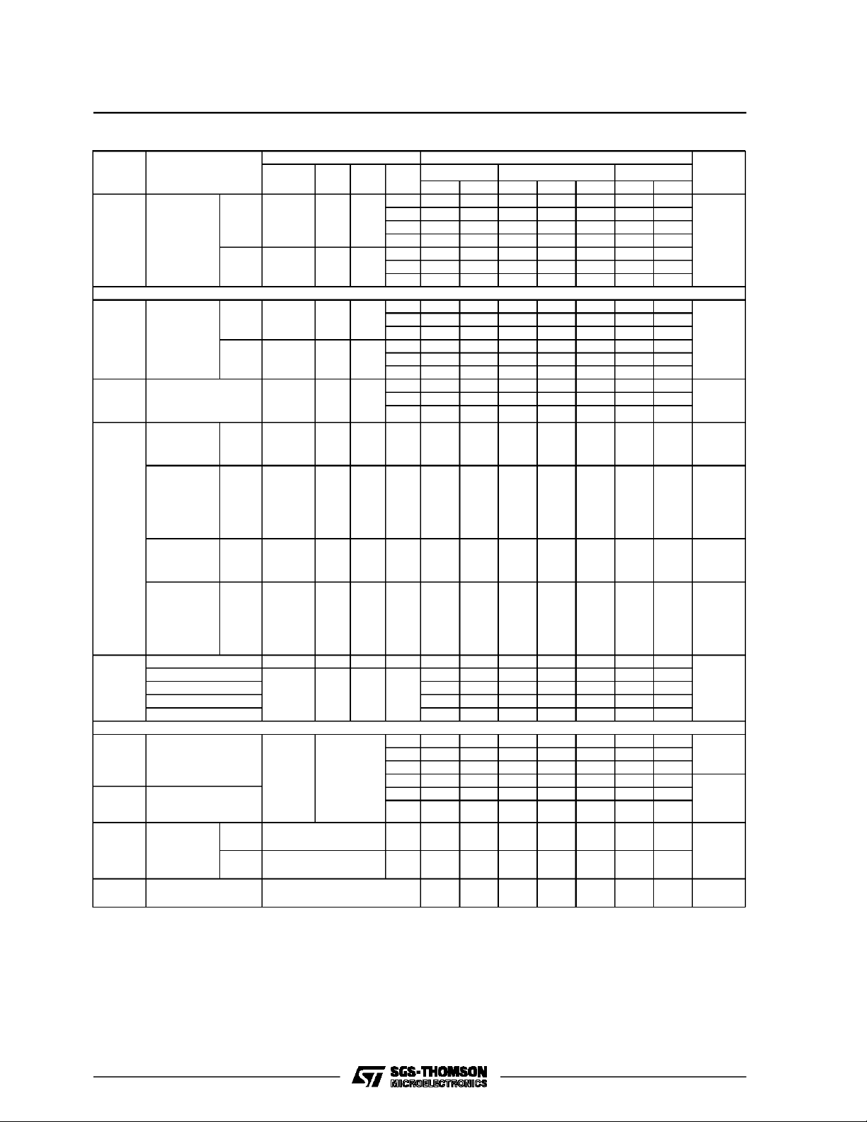
HCC/H CF4051B/52B/53B
STATIC ELECTRICAL CHARACTERISTICS (over recommended operating conditions)
Test Conditions Value
VEEVSSV
Symbol Parameter
IS
DD
V
(V) (V) (V) (V)
I
L
Quiescent
Device
Current
HCC
Types
HCF
Types
5 5 0.04 5 150
10 10 0.04 10 300
15 20 0.04 20 600
20 100 0.08 100 3000
5 20 0.04 20 150
10 40 0.04 40 300
15 80 0.04 80 600
SWIT CH
ON Resistance
∆ON Resistance ∆R
(between any 2
channels)
OFF (•)
Channel
Leakage
Current
Any
Channel
OFF
All
Channels
OFF
(common
HCC
Types
HCF
Types
HCC
Types
HCC
Types
ON
0 ≤ V
≤ V
DD
0 ≤ V
≤ V
DD
I
00
5 880 470 1050 1200
10 310 180 400 580
15 220 125 280 400
I
00
5 880 470 1050 1200
10 330 180 400 520
15 230 125 280 360
510
00
10 10
15 5
0 0 18 100 ± 0.1 100 1000 nA
0 0 18 100 ± 0.1 100 1000 nA
OUT/IN)
Any
Channel
OFF
HCF
Types
0 0 15 300 ± 0.1 300 1000 nA
All
Channels
OFF
(common
HCF
Types
0 0 15 300 ± 0.1 300 1000 nA
OUT/IN)
C
Input 5
Capaci-
tance
Output 4051
Output 4052 18
Output 4053 9
–5 –5 5
Feedthrough 0.2
CONTROL (Address or Inhibit)
V
V
I
IH,IIL
C
Input Low Voltage = V
IL
DD
Thru
1KΩ
Input High Voltage
IH
Input
Leakage
Current
HCC
Types
HCF
VI= 0/18V
= 0/15V
V
I
Types
Input Capacitance Any Address or Inhibit
I
V
EE=VSS
RL=1KΩ
to V
SS
IIS<2µA
(on all off
channels)
5 1.5 1.5 1.5
10 3 3 3
15 4 4 4
5 3.5 3.5 3.5
10 7 7 7
15 11 11 11
18 ± 0.1 ±10
15 ± 0.3 ±10
Input
(•) Determined by minimum feasible leakage measurement for automatic testing.
(*) T
(*) T
=–55°C for HCC device : – 40°CforHCF device.
Low
= + 125°CforHCC device : + 85°C for HCF device.
High
T
* 25 °CT
Low
Min. Max. Min. Typ. Max. Min. Max.
30
–3
± 0. 1 ± 1
–3
± 0. 3 ± 1
5 7.5 pF
High
*
Unit
µA
Ω
Ω
pF
V
V
µA
4/17

HCC/HCF4051B/52B/53B
DYNAMIC ELECTRICAL CHARACTERISTICS
(T
=25°C, CL= 50pF all input squarewave rise and fall time = 20ns)
amb
Test Conditions Valu e
Paramet e r
SWITCH
Propagation Delay Time
t
pd
(signal input to output)
Frequency Response
Channel ”ON” (sine wave
input)
at 20 Log = – 3dB
V
__
V
o
I
Feedthrough (all channels
OFF)
at 20 Log = – 40dB
V
__
V
o
I
Frequency Signal Crosstalk Between any 2 Channels 3
V
o
at 20 Log = – 40dB
__
V
I
Sine Wave Distortion
= 1kHz Sine Wave
f
is
CONTRO L (Address or Inhibit)
Progation Delay Time :
Address-to Signal OUT
Channels ON or OFF
Propagation Delay Time :
Inhibit to Signal OUT
(channel turning ON)
Propagation Delay Time :
Inhibit to Signal OUT
(channel turning OFF)
Address or Inhibit to Signal
Crosstalk
(•) Peak to peak voltage symmetrical about V
(*) Both ends of channel.
V
R
f
V
V
V
SS
DD
(V)
(V)
53030
10 15 60
(V)
EE
(kΩ)
200
L
i
(kHz)
IS
(V)
10 V
_
I__I
_
15 11 20
=V
15(•)10V
SS
at Common
o
OUT/IN
4053B 30
4052B 25
4051B 20
Voat any Channel 60
=V
15(•)10V
SS
at Common
o
OUT/IN
4053 8
4052 10
4051 12
Voat any Channel 8
=VSS15(•) 10 Between Sections
4052B only
measured
on
common
measured
onany
channel
Between any 2
Sections 4053B
only
in Pin 2
out Pin 1 4
in Pin 15
out Pin 1 4
=VSS10 1 2 (•) 5 0.3
10 1 3 (•) 10 0.2
10 1 5 (•) 15 0.12
0 0 5 360 720
0 0 10 160 320
0 0 15 120 240
–5 0 5 225 450
0
0 0 10 160 320
10
0 0 15 120 240
05 360720
– 10 0 5 200 400
0
010 90210
0.3
015 70160
5 200 450
–10 5 130 300
0 10* 0 10
DD-VEE
2
V
C=VDD–VSS
wave)
(square
Typ. Max.
6
10
2.5
6
65
Unit
ns
MHz
MHz
MHz
MHz
%
ns
ns
ns
mV
peak
5/17

HCC/H CF4051B/52B/53B
Typical Channel ON Resistance vs. Input Signal
Voltage(all types).
Typical Channel ON Resistance vs. Input Signal
Voltage(all types).
Typical Channel ON Resistance vs. Input Signal
Voltage (all types).
Typical Channel ON Resistance vs. Input Signal
Voltage (all types).
TypicalDynamic PowerDissipation/Package vs.Switching Frequency and TestCircuit(4051B).
6/17

HCC/HCF4051B/52B/53B
Typical ON Characteristics for 1 of 8 Channels
(4051B).
Typical DynamicPower Dissipation/Package vs. Switching Frequency andTest Circuit (4052B).
Typical DynamicPower Dissipation/Package vs. Switching Frequency andTest Circuit (4053B).
7/17

HCC/H CF4051B/52B/53B
WAVEFORMS
ChannelBeing Turned ON (RL=10KΩ). Channel Being Turned OFF(RL=300KΩ).
TYPICAL BIAS VOLTAGES
Fig. (a) Fig. (b) Fig.(c) Fig. (d)
The ADDRESS (digital-control inputs) and INHIBIT logic levels are : ”0”=VSSand ”1”=VDD. The analog signal (trough the TG)
may swing from VEEto VDD.
8/17

TYPICAL APPLICATIONS
TYPICALTIME-DIVISION APPLICATION OFTHE 4052B
HCC/HCF4051B/52B/53B
SPECIAL CONSIDERATIONS
Control of analog signals up to 20V peak-to-peak
can be achieved bydigital signal amplitudes of 4.5
to 20V(if VDD–VSS=3V,a VDD–VEEofup to 13V
can be controlled ; for VDD–VEElevel differences
above13V,a VDD–VSSofat least 4.5Visrequired).
For example, if VDD= +5V, VSS= 0, and VEE=
–13.5V, analog signals from – 13.5V to + 4.5V can
be controlledby digital inputs of 0to 4.5V. Incertain
applications, the externalload-resistor current may
include both VDDand signal-line components. To
avoid drawing VDDcurrent when switch current
flowsinto the transmission gate inputs,the voltage
dropacrossthebidirectional switchmustnotexceed
0,8 volt (valvulated from RONvalues shown in
ELECTRICAL CHARACTERISTICS CHART). No
VDDcurrent willflow through RLif the switch current
flowsinto lead3 ontheHCC/HCF4051; leads3and
13 on the HCC/HCF4052 ; leads 4, 14, and 15 on
the HCC/HCF4053.
9/17

HCC/H CF4051B/52B/53B
TEST CIRCUITS
Off ChannelLeakage Current-any Channel OFF.
4051 4052 4053
Off ChannelLeakage Current-all Channel OFF.
4051 4052
Propagation Delay-adress Input to SignalOutput.
4051
4052
4053
4053
10/17

TEST CIRCUITS (continued)
Propagation Delay-Inhibit Inputto Signal Output.
4051 4052 4053
Input Voltage.
HCC/HCF4051B/52B/53B
4051 4052
4053
QuiescentDevice Current. ChannelON Resistance
Meaurement Circuit.
4051
4053
4052
11/17

HCC/H CF4051B/52B/53B
TEST CIRCUITS (continued)
Input Current.
40524051 - 4053
CrosstalkBetwen any two Channels (All Types).
Feedthrough (All Types).
Crosstalk Betweenn Duals or Triplets (4052-4053).
12/17

HCC/HCF4051B/52B/53B
Plastic DIP16 (0.25) MECHANICAL DATA
DIM.
MIN. TYP. MAX. MIN. TYP. MAX.
a1 0.51 0.020
B 0.77 1.65 0.030 0.065
b 0.5 0.020
b1 0.25 0.010
D 20 0.787
E 8.5 0.335
e 2.54 0.100
e3 17.78 0.700
F 7.1 0.280
I 5.1 0.201
L 3.3 0.130
Z 1.27 0.050
mm inch
P001C
13/17

HCC/H CF4051B/52B/53B
Ceramic DIP16/1 MECHANICAL DATA
DIM.
MIN. TYP. MAX. MIN. TYP. MAX.
A 20 0.787
B 7 0.276
D 3.3 0.130
E 0.38 0.015
e3 17.78 0.700
F 2.29 2.79 0.090 0.110
G 0.4 0.55 0.016 0.022
H 1.17 1.52 0.046 0.060
L 0.22 0.31 0.009 0.012
M 0.51 1.27 0.020 0.050
N 10.3 0.406
P 7.8 8.05 0.307 0.317
Q 5.08 0.200
mm inch
14/17
P053D

HCC/HCF4051B/52B/53B
SO16 (Narrow) MECHANICAL DATA
DIM.
MIN. TYP. MAX. MIN. TYP. MAX.
A 1.75 0.068
a1 0.1 0.2 0.004 0.007
a2 1.65 0.064
b 0.35 0.46 0.013 0.018
b1 0.19 0.25 0.007 0.010
C 0.5 0.019
c1 45° (typ.)
D 9.8 10 0.385 0.393
E 5.8 6.2 0.228 0.244
e 1.27 0.050
e3 8.89 0.350
F 3.8 4.0 0.149 0.157
G 4.6 5.3 0.181 0.208
L 0.5 1.27 0.019 0.050
M 0.62 0.024
S8°(max.)
mm inch
P013H
15/17

HCC/H CF4051B/52B/53B
PLCC20 MECHANICAL DATA
DIM.
MIN. TYP. MAX. MIN. TYP. MAX.
A 9.78 10.03 0.385 0.395
B 8.89 9.04 0.350 0.356
D 4.2 4.57 0.165 0.180
d1 2.54 0.100
d2 0.56 0.022
E 7.37 8.38 0.290 0.330
e 1.27 0.050
e3 5.08 0.200
F 0.38 0.015
G 0.101 0.004
M 1.27 0.050
M1 1.14 0.045
mm inch
16/17
P027A

HCC/HCF4051B/52B/53B
Information furnished is believed tobe accurate and reliable.However, SGS-THOMSON Microelectronicsassumes no responsability forthe
consequences of useof such information nor for any infringement of patents or other rights of third parties which may results from itsuse. No
license isgranted by implication or otherwise under any patent orpatent rights ofSGS-THOMSON Microelectronics. Specificationsmentioned
in this publication are subject to changewithout notice. This publication supersedesand replaces all information previously supplied.
SGS-THOMSON Microelectronicsproducts are not authorized foruse ascritical componentsin life support devices or systemswithout express
written approval of SGS-THOMSONMicroelectonics.
1994 SGS-THOMSON Microelectronics - All RightsReserved
Australia - Brazil - France - Germany- HongKong - Italy - Japan - Korea- Malaysia - Malta -Morocco - The Netherlands-
Singapore - Spain - Sweden - Switzerland - Taiwan - Thailand - UnitedKingdom - U.S.A
SGS-THOMSON Microelectronics GROUP OF COMPANIES
17/17
 Loading...