

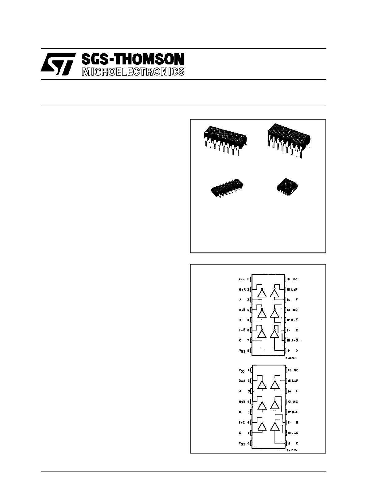
4049UB INVERT I NG TYPE
4050B NON-INVERT ING TYPE
. HIGH SINK CURRENT FOR DRIVING 2 TTL
LOADS
.HIGH-TO-LOWLEVEL LOGIC CONVERSION
.QUIESCENT CURRENT SPECIFIED TO 20V
FOR HCC DEVICE
.HIGH ”SINK” AND ”SOURCE” CURRENT CA-
PABILITY
.5V, 10VAND 15V PARAMETRIC RATINGS
.INPUTCURRENTOF100 nA AT18V AND25°C
FOR HCC DEVICE
.100% TESTEDFOR QUIESCENTCURRENT
.MEETSALLREQUIREMENTSOFJEDECTEN-
TATIVE STANDARD No. 13A, ”STANDARD
SPECIFICATIONSFOR DESCRIPTIONOF ”B”
SERIESCMOS DEVICES”
HCC/HCF4049UB
HCC/HCF4050B
HEX BUFFER/CONVERTERS
EY
(PlasticPackage)
M1
(MicroPackage)
ORDERCODES :
HCC40XXBF HCF40XXBM1
HCF40XXBEY HCF40XXBC1
(Ceramic Frit Seal Package)
(Plastic ChipCarrier)
F
C1
DESCRI PTIO N
The HCC4049UB/4050B (extended temperature
range) and the HCF4049UB/4050B (intermediate
temperature range) are monolithic integrated circuits available in 16-lead dual in-line plastic or ceramic package andplastic micro package.
The HCC/HCF4049UB/4050B are inverting and
non-inverting hex buffers, respectively, and feature
logic-level conversion usingonlyonesupply voltage
(VDD). Theinput-signal high level(VIH) can exceed
theVDDsupplyvoltage when thesedevicesareused
for logic level conversions. These devices are intendedforuse asCOS/MOSto DTL/TTLconverters
andcandrivedirectlytwoDTL/TTLloads(VDD=5V,
VOL≤ 0.4V, and IOL≥ 3.2mA).
PIN CONNE CT I ON S
4049UB
4050B
June 1989
1/12
HCC/H CF4049UB/4050B
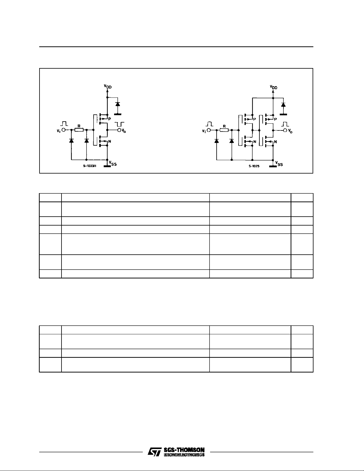
SCHEM ATIC D IA G RA MS ( 1 of 6 ident i c al units)
4049UB 4050B
ABSOLUTE M AXI MUM RATI N GS
Symbol Parameter Value Unit
V
* Supply Voltage : HCC Types
DD
HCF Types
V
Input Voltage – 0.5 to VDD+ 0.5 V
i
I
DC Input Current (any one input) ± 10 mA
I
P
Total Power Dissipation (per package)
tot
Dissipation per Output Transistor
for Top= Full Package-temperature Range
T
Operating Tem perature : HCC Types
op
HCF Types
T
Stresses above those listed under ”Absolute Maximum Ratings” may cause permanent damage to the device. This is a stress
rating only and functional operation of the device at these or any other conditions above those indicated in the operational sections of this specification is not implied. Exposure to absolute maximum rating conditions for external periods may affect device
reliability.
*
Allvoltage values are referred to VSSpinvoltage.
Storage Temperature – 65 to + 150 °C
stg
– 0.5 to + 20
– 0.5 to + 18
200
100
– 55 to + 125
–40to+85
V
V
mW
mW
°C
°C
RECOMMENDED OPERATING CONDITIONS
Symbol Parameter Value Unit
V
T
2/12
Supply Voltage :HC C Types
DD
HCF Types
V
Input Voltage 0 to V
I
Operating Tem perature : HCC Types
op
HCF Types
3to18
3to15
DD
– 55 to + 125
–40to+85
V
V
V
°C
°C
HCC/HCF4049UB/4050B
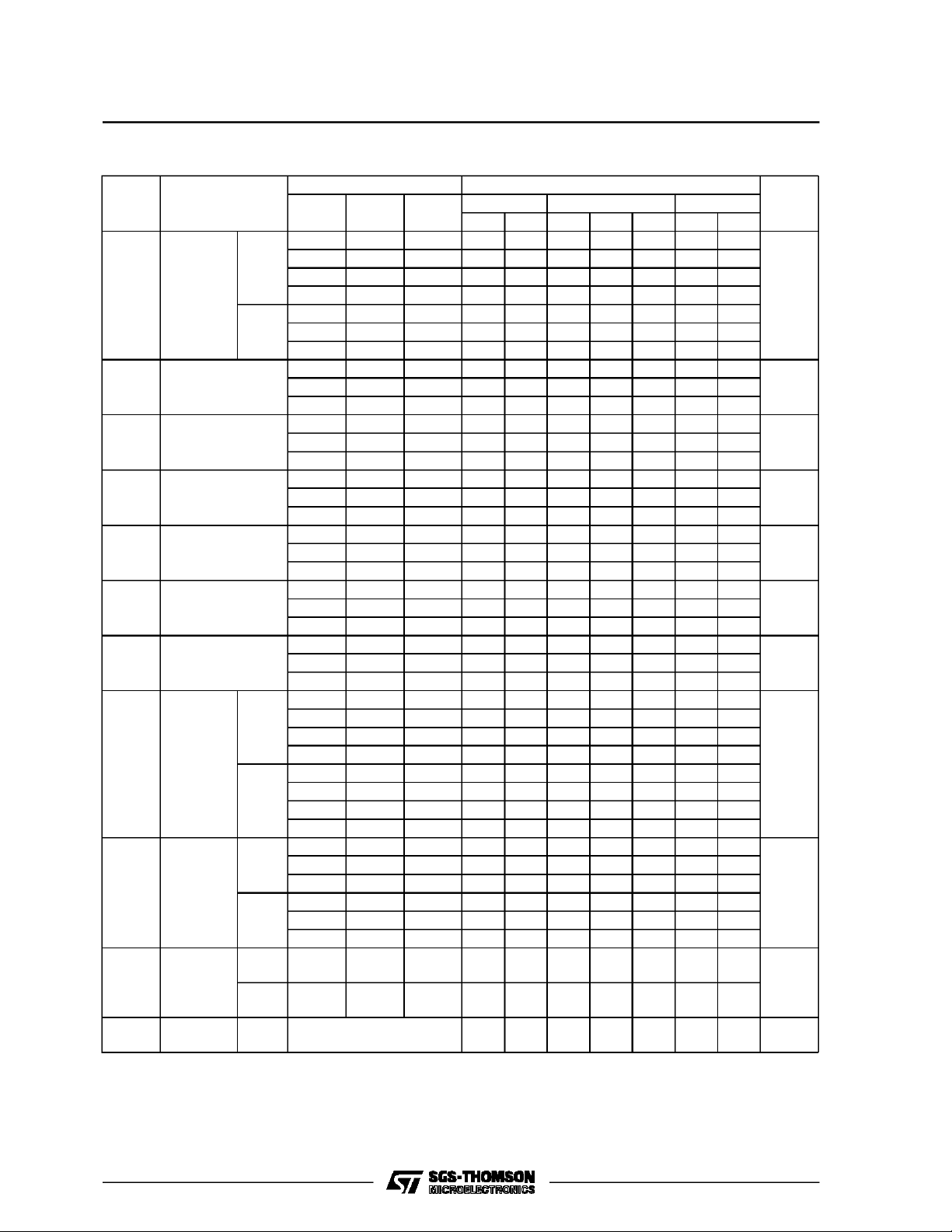
STATIC ELECTRICAL CHARACTERISTICS (over recommended operatingconditions)
Test Conditions Value
Symbo l Parameter V
I
L
Quiescent
Supply
Current
HCC
Types
0/ 5 5 1 0.02 1 30
0/10 10 2 0.02 2 60
0/15 15 4 0.02 4 120
(V) (V) (V)
V
I
0/20 20 20 0.04 20 600
0/ 5 5 4 0.02 4 30
0/10 10 8 0.02 8 60
0/15 15 16 0.02 16 120
0/ 5 5 4.95 4.95 4.95
0/10 10 9.95 9.95 9.95
V
OH
HCF
Types
Output High
Voltage
0/15 15 14.95 14.95 14.95
V
OL
Output Low
Voltage
5/0 5 0.05 0.05 0.05
10/0 10 0.05 0.05 0.05
15/0 15 0.05 0.05 0.05
Input High
V
IH
Voltage (4049UB)
0.5 5 4 4 4
1108 8 8
21512 12 12
V
IH
Input High
Voltage (4050B)
4.5 5 3.5 3.5 3.5
9107 7 7
13.5 16 11 11 11
Input Low
V
IL
Voltage (4049UB)
4.5 5 1 1 1
910 2 2 2
13 15 3 3 3
V
IL
Input Low
Voltage (4050B)
0.5 5 1.5 1.5 1.5
110 3 3 3
1.5 15 4 4 4
Output
I
OH
Drive
Current
HCC
Types
0/ 5 2.5 5 1.6 –1.25 – 6.4 – 0.9
0/ 5 4.6 5 0.64 –0.51 – 1.6 –0.36
0/10 9.5 10 1.6 –1.30 – 3.6 – 0.9
0/15 13.5 15 4.7 –3.75 – 12 – 2.7
0/ 5 2.5 5 1.5 –1.25 – 6.4 – 1
HCF
Types
0/ 5 4.6 5 0.61 –0.51 – 1.6 –0.42
0/10 9.5 10 1.5 –1.25 – 3.6 – 1
0/15 13.5 15 4.5 –3.75 – 12 – 3
Output
I
OL
Sink
Current
HCC
Types
HCF
Types
I
IH,IIL
Input
Leakage
Current
HCC
Types
HCF
Types
C
Input
I
Capacitance
(*) T
=–55°C for HCC device : – 40°CforHCF device.
Low
T
= + 125°CforHCC device : + 85°CforHCF device.
High
The Noise Margin (only HCC/HCF4050B type) for both ”1” and ”0” level is : 1V min. with VDD= 5V, 2V min. with VDD= 10V,
2.5V min. with VDD= 15V.
4049UB
4050B
0/ 5 0.4 5 3.75 3.2 6.4 2.2
0/10 0.5 10 10 8 16 5.6
0/15 1.5 15 30 24 48 17
0/ 5 0.4 5 3.6 3.2 6.4 2.6
0/10 0.5 10 9.6 8 16 6.6
0/15 1.5 15 28 24 48 19
0/18 18 ± 0.1 ±10
0/15 15 ± 0.3 ±10
Any Input
V
O
DD
T
* 25° CT
Low
High
* Unit
Min. Max. Min. Typ. Max. Min. Max.
µA
V
V
V
V
V
V
mA
mA
–5
± 0. 1 ± 1
–5
± 0. 3 ± 1
15522.5
7.5
µA
pF
3/12
HCC/H CF4049UB/4050B
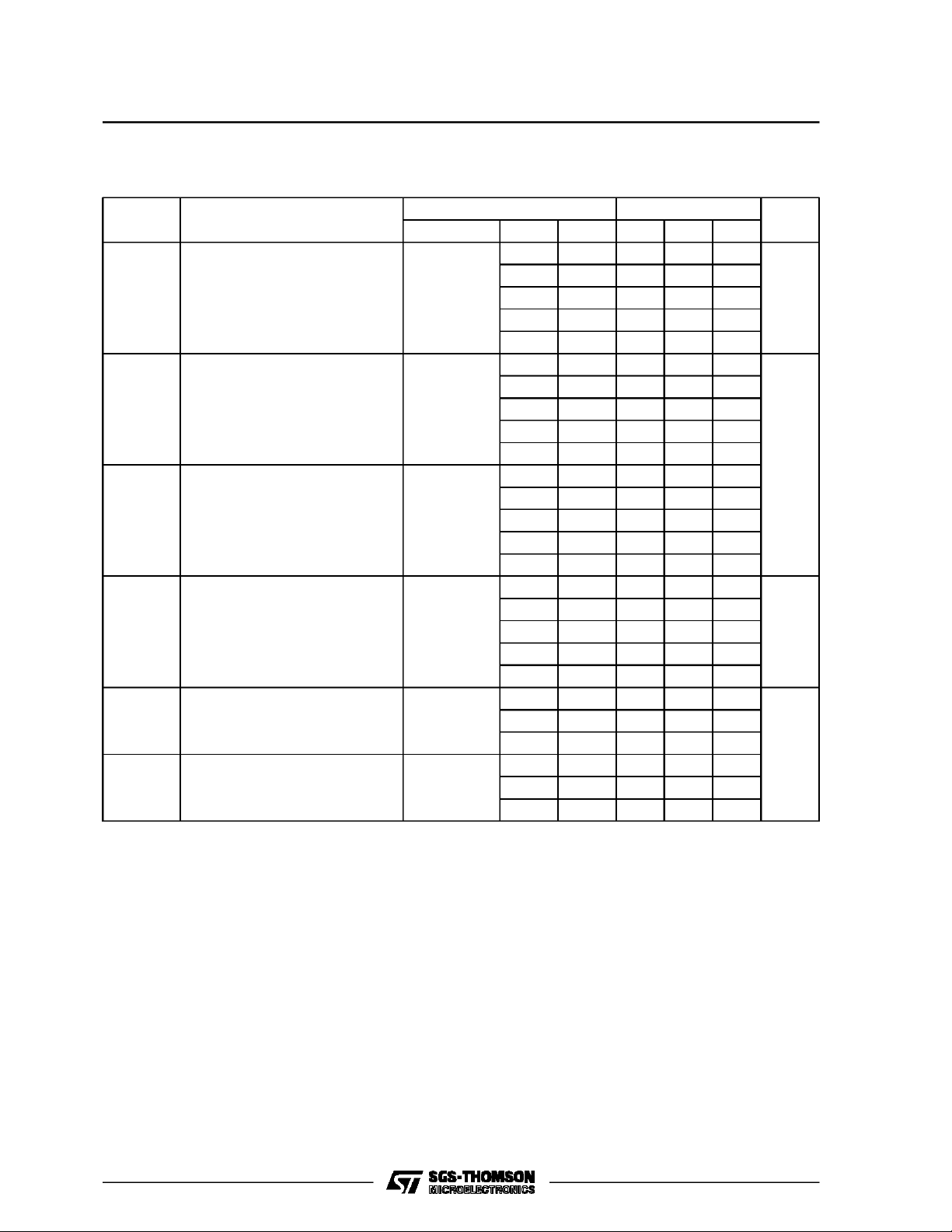
DYNAMIC ELECTRICAL CHARACTERISTICS (T
=25°C, CL= 50pF, RL= 200kΩ,
amb
typical temperature coefficient for all VDDvalues is 0.3%/°C, all input rise andfall times = 20ns)
Symbol Parameter
t
PL H
Propagation Delay Time
(4049UB)
t
PL H
Propagation Delay Time
(4050B)
t
PHL
Propagation delay Time
(4049UB)
t
PHL
Propagation Delay Time
(4050B)
t
t
TLH
THL
Transition Time 5 5 80 160
Transition Time 5 5 30 60
Test Conditions Value
V
(V) VDD(V) Min. Typ. Max.
I
5 5 60 120
10 10 32 65
10 5 45 90
15 15 25 50
15 5 45 90
5 5 70 140
10 10 40 80
10 5 45 90
15 15 30 60
15 5 40 80
55 3265
10 10 20 40
10 5 15 30
15 15 15 30
15 5 10 20
5 5 55 110
10 10 22 55
10 5 50 100
15 15 15 30
15 5 50 100
10 10 40 80
15 15 30 60
10 10 20 40
15 15 15 30
Unit
ns
ns
ns
ns
4/12

HCC/HCF4049UB/4050B
Minimum and Maximum Voltage Transfer Characteristicsfor 4049UB.
TypicalVoltage Transfer Characteristics as a Function ofTemperature for 4049UB.
Minimum and Maximum VoltageTransfer Characteristicsfor 4050B.
TypicalVoltage TransferCharacteristics asa Function ofTemperature for 4050B.
TypicalOutputLow (sink)Current Characteristics. MinimumOutputLow(sink) CurrentCharacteristics.
5/12

HCC/H CF4049UB/4050B
Typical Output High (source) Current Characteristics.
Typical Power Dissipation per Buffer/Inverter vs.
Frequency.
Minimum Output High (source) Current Characteristics.
TypicalPower Dissipation vs.InputTransition Time
per Inverter for 4049UB.
TypicalPower Dissipation vs.Input Transition Time
perInverter for 4050B.
6/12
Logic-Level Conversion Application.

TEST CIRCUITS
QuiescentDevice Current. Input Voltage.
Input Current.
HCC/HCF4049UB/4050B
7/12

HCC/H CF4049UB/4050B
Plastic DIP16 (0.25) MECHANICAL DATA
DIM.
MIN. TYP. MAX. MIN. TYP. MAX.
a1 0.51 0.020
B 0.77 1.65 0.030 0.065
b 0.5 0.020
b1 0.25 0.010
D 20 0.787
E 8.5 0.335
e 2.54 0.100
e3 17.78 0.700
F 7.1 0.280
I 5.1 0.201
L 3.3 0.130
Z 1.27 0.050
mm inch
8/12
P001C

HCC/HCF4049UB/4050B
Ceramic DIP16/1 MECHANICAL DATA
DIM.
MIN. TYP. MAX. MIN. TYP. MAX.
A 20 0.787
B 7 0.276
D 3.3 0.130
E 0.38 0.015
e3 17.78 0.700
F 2.29 2.79 0.090 0.110
G 0.4 0.55 0.016 0.022
H 1.17 1.52 0.046 0.060
L 0.22 0.31 0.009 0.012
M 0.51 1.27 0.020 0.050
N 10.3 0.406
P 7.8 8.05 0.307 0.317
Q 5.08 0.200
mm inch
P053D
9/12

HCC/H CF4049UB/4050B
SO16 (Narrow) MECHANICAL DATA
DIM.
MIN. TYP. MAX. MIN. TYP. MAX.
A 1.75 0.068
a1 0.1 0.2 0.004 0.007
a2 1.65 0.064
b 0.35 0.46 0.013 0.018
b1 0.19 0.25 0.007 0.010
C 0.5 0.019
c1 45° (typ.)
D 9.8 10 0.385 0.393
E 5.8 6.2 0.228 0.244
e 1.27 0.050
e3 8.89 0.350
F 3.8 4.0 0.149 0.157
G 4.6 5.3 0.181 0.208
L 0.5 1.27 0.019 0.050
M 0.62 0.024
S8°(max.)
mm inch
10/12
P013H

PLCC20 MECHANICAL DATA
HCC/HCF4049UB/4050B
DIM.
MIN. TYP. MAX. MIN. TYP. MAX.
A 9.78 10.03 0.385 0.395
B 8.89 9.04 0.350 0.356
D 4.2 4.57 0.165 0.180
d1 2.54 0.100
d2 0.56 0.022
E 7.37 8.38 0.290 0.330
e 1.27 0.050
e3 5.08 0.200
F 0.38 0.015
G 0.101 0.004
M 1.27 0.050
M1 1.14 0.045
mm inch
P027A
11/12

HCC/H CF4049UB/4050B
Information furnished is believed tobe accurate and reliable.However, SGS-THOMSON Microelectronicsassumes no responsability forthe
consequences of useof such information nor for any infringement of patents orother rights of third partieswhich may results from its use. No
license isgranted by implication or otherwiseunder any patent or patent rights ofSGS-THOMSON Microelectronics. Specificationsmentioned
in this publication are subject to changewithout notice. This publication supersedesand replaces all information previously supplied.
SGS-THOMSON Microelectronicsproductsare notauthorized foruse ascriticalcomponentsin life support devices orsystems withoutexpress
written approval of SGS-THOMSONMicroelectonics.
1994 SGS-THOMSON Microelectronics - All RightsReserved
Australia - Brazil - France - Germany- HongKong - Italy - Japan - Korea - Malaysia - Malta -Morocco - The Netherlands-
Singapore - Spain - Sweden - Switzerland - Taiwan - Thailand - UnitedKingdom - U.S.A
SGS-THOMSON Microelectronics GROUP OF COMPANIES
12/12
 Loading...