

MULTIFUNCTION EXPANDABLE 8-INPUT GATE
.THREE-STATEOUTPUT
.MANY LOGIC FUNCTIONS AVAILABLE IN
ONE PACKAGE
.QUIESCENT CURRENT SPECIFIED TO 20V
FOR HCC DEVICE
.STANDARDIZED SYMMETRICAL OUTPUT
CHARACTERISTICS
.5V, 10V,AND 15VPARAMETRIC RATINGS
.INPUT CURRENTOF100nAAT 18V AND 25°C
FOR HCC DEVICE
.100% TESTEDFOR QUIESCENT CURRENT
.MEETSALLREQUIREMENTSOFJEDECTEN-
TATIVE STANDARD N°. 13A, ”STANDARD
SPECIFICATIONS FOR DESCRIPTIONOF ”B”
SERIESCMOS DEVICES”
HCC/HCF4048B
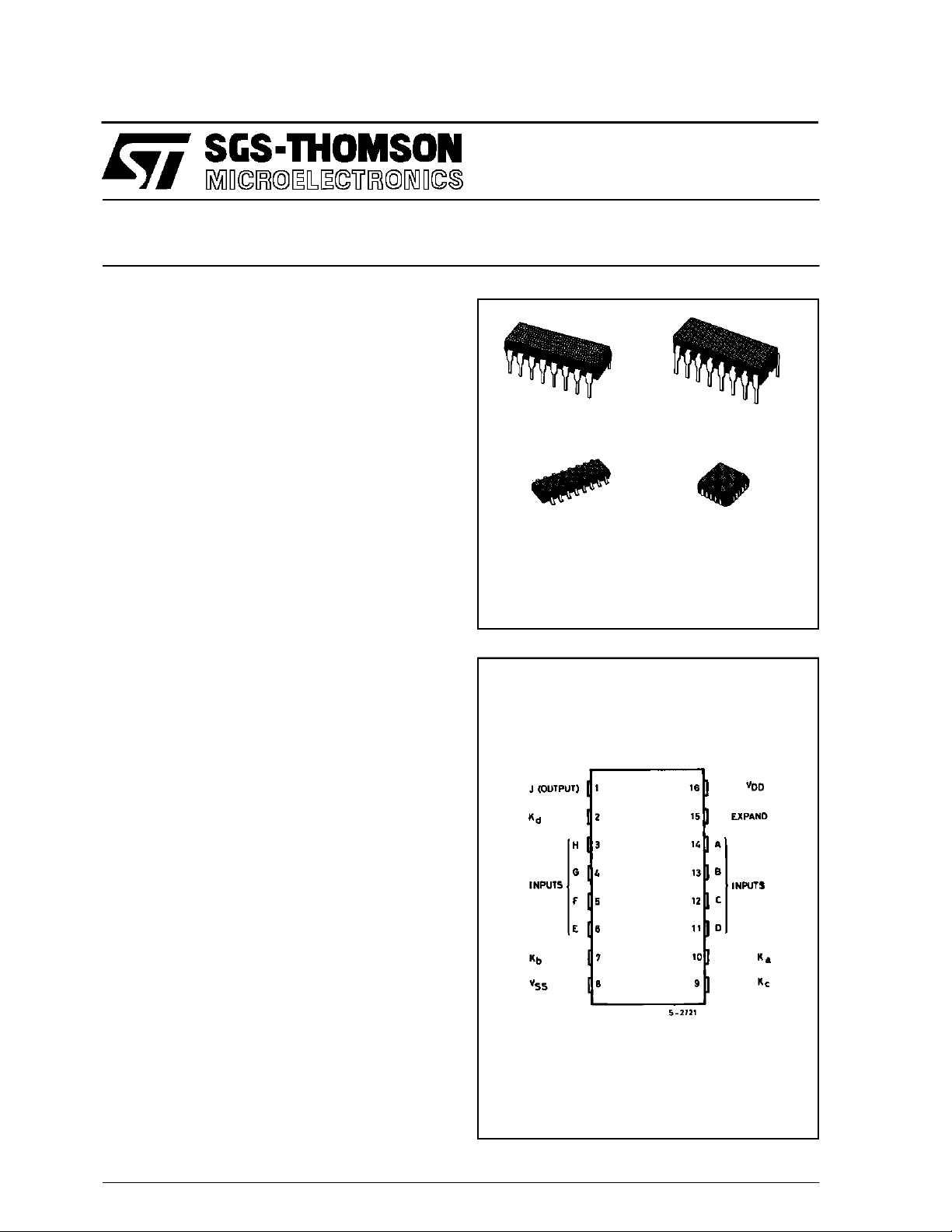
EY
PlasticPackage
M1
MicroPackage
ORDER CODES :
HCC4048BF HCF4048BM1
HCF4048BEY HCF4048BC1
Ceramic FritSealPackage
Plastic ChipCarrier
F
C1
DESCRIP TI O N
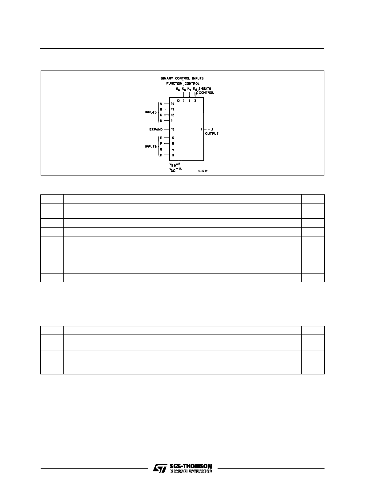
The HCC4048B (extended temperature range) and
HCF4048B (intermediate temperature range) are
monolithic integrated circuit, available in 16-lead
dual in-line plastic or ceramic package and plastic
micro package. The HCC/HCF4048B is an 8-input
gate having four controlinputs. Threebinary control
inputs-Ka,Kb, andKc- provide the implementation
ofeightdifferent logicfunctions.Thesefunctionsare
OR, NOR, AND, NAND, OR/AND, OR/NAND,
AND/OR and AND/NOR.A fourth control input-Kdprovidestheuserwitha3-stateoutput.Whencontrol
inputKdis hightheoutputiseitheralogic1 oralogic
0 depending on the inner states. When control input
Kd is low, the output isan opencircuit. This feature
enables the usertoconnectthisdevicetoacommon
bus line. In addition to theeight input lines, an EXPAND input is provided that permits the user to increase thenumber ofinputs tooneHCC/HCF4048B.
For example, two HCC/HCF4048B’s can be cas-
caded toprovidea 16-input multifunction gate.When
the EXPAND input is not used, it should be connected to VSS.
PIN CON NECTI O N S
October 1988
1/12
HCC/HCF4048B
FUN CTIONAL DIAGR A M
ABSOLUTE MAXIMUM RAT I N GS
Symbol Parameter Value Unit
V
* Supply Voltage :HCC Types
DD
HCF Types
V
Input Voltage – 0.5 to VDD+ 0.5 V
i
I
DC Input Current (any one input) ± 10 mA
I
P
Total Power Dissipation (per package)
tot
Dissipation per Output Transistor
for T
T
Operating Temperature : HCC Types
op
= Full Package-temperature Range
op
HCF Types
T
Stresses above those listed under ”Absolute Maximum Ratings” may cause permanent damage to the device. This is a stress rating only
and functional operation of the device atthese orany other conditions above those indicated inthe operational sections of this specification
is not implied. Exposure to absolute maximum rating conditions for external periods may affect device reliability.
* All voltages values are referred to VSSpin voltage.
Storage Temperature – 65 to + 150 °C
stg
– 0.5 to + 20
– 0.5 to + 18
200
100
– 55 to + 125
–40to+85
V
V
mW
mW
°C
°C
RECOMMENDED OPERATING CONDITIONS
Symbol Parameter Value Unit
2/12
V
Supply Voltage :HCC Types
DD
HCF Types
V
Input Voltage 0 to V
I
T
Operating Temperature : HCC Types
op
HCF Types
3to18
3to15
DD
– 55 to + 125
–40to+85
V
V
V
°C
°C

BASIC LOGIC CON FIGURATIONS
LOGI C DI AG RAM
HCC/HCF4048B
FUNCTION TRUTH TABLE
Output Function Boolean Expression KaKbK
NOR
OR
OR/AND
OR/NAND
AND
NAND
AND/NOR
AND/OR
Kd=1
K
EXPAND Input = 0
Normal Inverter Action
=0
High Impedance Output
d
J=A+B+C+D+E+F+G+H
J=A+B+C+D+E+F+G+H
J=(A+B+C+D)•(E+F+G+H)
J=(A+B+C+D)•(E+F+G+H)
J = ABCDEFGH
J = ABCDEFGH
J = ABCD+EFGH
J = ABCD + EFGH
0
0
0
0
0
1
0
1
1
0
1
0
1
1
1
1
Unused Input
c
0
1
0
1
0
1
0
1
V
SS
V
SS
V
SS
V
SS
V
DD
V
DD
V
DD
V
DD
3/12
HCC/HCF4048B
STATIC ELECTRICAL CHARACTERISTICS (over recommended operating conditions)
Symbol Parameter
Quiescent
I
L
Current
HCC
Types
HCF
Types
OH
Output High
V
Voltage
OL
Output Low
V
Voltage
V
IH
Input High
Voltage
IL
Input Low
V
Voltage
I
OH
Output
Drive
Current
HCC
Types
HCF
Types
OL
Output
Sink
Current
HCC
Types
I
HCF
Types
I
IH,IIL
Input
Leakage
Current
HCC
Types
HCF
Types
I
OH
3-state
Output
Current
HCC
Types
HCF
Types
C
I
*T
=–55°C for HCC device : – 40°C for HCF device.
LOW
*T
= – 125°CforHCC device : – 85°CforHCF device.
HIGH
The Noise Margin for both ”1” and ”0” level is : 1V min. with VDD= 5V, 2V min. with VDD= 10V, 2.5V min. with VDD= 15V,
Input Capacitance Any Input 5 7.5 pF
Test Conditions Value
V
V
I
(V) (V) (µA) (V)
O
|IO|V
T
DD
* 25°CT
Low
Min. Ma x. Min. Typ. M ax. Min. Max .
High
0/ 5 5 0.25 0.01 0.25 7.5
0/10 10 0.5 0.01 0.5 15
0/15 15 1 0.01 1 30
0/20 20 5 0.02 5 150
0/ 5 5 1 0.01 1 7.5
0/10 10 2 0.01 2 15
0/15 15 4 0.01 4 30
0/ 5 < 1 5 4.95 4.95 4.95
0/10 < 1 10 9.95 9.95 9.95
0/15 < 1 15 14.95 14.95 14.95
5/0 < 1 5 0.05 0.05 0.05
10/0 < 1 10 0.05 0.05 0.05
15/0 < 1 15 0.05 0.05 0.05
0.5/4.5 < 1 5 3.5 3.5 3.5
1/9 < 1 10 7 7 7
1.5/13.5 < 1 15 11 11 11
4.5/0.5 < 1 5 1.5 1.5 1.5
9/1 < 1 10 3 3 3
13.5/1.5 < 1 15 4 4 4
0/ 5 2.5 5 – 2 – 1.6 – 3.2 – 1.15
0/ 5 4.6 5 – 0.64 – 0.51 – 1 – 0.36
0/10 9.5 10 – 1.6 – 1.3 – 2.6 – 0.9
0/15 13.5 15 – 4.2 – 3.4 – 6.8 – 2.4
0/ 5 2.5 5 – 1.53 – 1.36 – 3.2 – 1.1
0/ 5 4.6 5 – 0.52 – 0.44 – 1 – 0.36
0/10 9.5 10 – 1.3 – 1.1 – 2.6 – 0.9
0/15 13.5 15 – 3.6 – 3.0 – 6.8 – 2.4
0/ 5 0.4 5 0.64 0.51 1 0.36
0/10 0.5 10 1.6 1.3 2.6 0.9
0/15 1.5 15 4.2 3.4 6.8 2.4
0/ 5 0.4 5 0.52 0.44 1 0.36
0/10 0.5 10 1.3 1.1 2.6 0.9
0/15 1.5 15 3.6 3.0 6.8 2.4
0/18
18 ± 0.1 ± 10
-5
± 0.01 ± 1
Any Input
0/15
15 ± 0.3 ± 10
0/18 0/18 18 ± 0.4 ± 10
0/15 0/15 15 ± 1.0 ± 10
-5
± 0.3 ± 1
-4
± 0.4 ± 12
-4
± 1.0 ± 7.5
Unit
*
µA
V
V
V
V
mA
mA
µA
µA
4/12

HCC/HCF4048B
DYNAMIC ELECTRICAL CHARACTERISTICS (T
=25°C, CL= 50pF, RL= 200kΩ,
amb
typical temperature coefficient for all VDD= 0.3%/°C values, all input rise and fall time = 20ns)
Symbol Parameter
t
PHL,tPLH
Propagation Delay Time Inputs
to Output and Ka to Output
Kb to Output 5 225 450
Kc to Output 5 140 280
Expand Input to Output 5 190 380
t
PHZ,tPL Z
t
PZH,tPZL
t
THL,tTL H
3–state Propagation Delay Time
Kd to Output
Transition Time 5 100 200
3-state Output Capacitance 5 10 pF
Test Con di t i on s Value
V
(V) Min. Typ. Max.
DD
5300600
10 150 300
15 120 240
10 85 170
15 55 110
10 50 100
15 40 80
10 90 180
15 65 130
RL=1kΩ 580160
10 35 70
15 25 50
10 50 100
15 40 80
Unit
ns
TypicalOutputLow (sink) Current Characteristics. MinimumOutputLow(sink) CurrentCharacteristics.
5/12

HCC/HCF4048B
Typical Output High (source) Current Characteristics.
Minimum Output high (source) Current Characteristics.
APPLICATIONS OF EXPAND INPUT
ACTUAL-CIRCUIT LOGIC CONFIGURATIONS EXPANSION LOGIC AND TRUTH TABLE
IMPLEMENTATION OF EXPAND INPUT
FOR 9 OR MORE INPUTS
OUTPUT
FUNCTION
NOR OR J = (A+B+C+D+E+F+G+H)+ (EXP)
OR OR J = (A+B+C+D+E+F+G+H) + (EXP)
AND NAND J =(ABCDEFGH)⋅ (EXP)
NAND NAND J = (ABCDEFGH)⋅ (EXP)
OR/AND NOR J = (A+B+C+D)⋅ (E+F+G+H)⋅ (EXP)
OR/NAND NOR J =(A+B+C+D)⋅ (E+F+G+H)⋅ (EXP)
AND/NOR AND J =(ABCD)+ (EFGH) + (EXP)
AND/OR AND J =(ABCD)+ (EFGH)+(EXP)
Note :(EXP)designatesthe EXPANDfunction(i.e., X1+X2+..XN).
FUNCTION
NEEDEDAT
EXPANDINPUT
OUTPUTBOOLEANEXPRESSION
6/12

APPLICATIONS OF EXPAND INPUT (cont inued )
12-Input or/and Gate. 16-Input Nor Gate.
TEST CIRCUITS
HCC/HCF4048B
Input Current.
Input Voltage.QuiescentDevice Current.
7/12

HCC/HCF4048B
Plastic DIP16 (0.25) MECHANICAL DATA
DIM.
MIN. TYP. MAX. MIN. TYP. MAX.
a1 0.51 0.020
B 0.77 1.65 0.030 0.065
b 0.5 0.020
b1 0.25 0.010
D 20 0.787
E 8.5 0.335
e 2.54 0.100
e3 17.78 0.700
F 7.1 0.280
I 5.1 0.201
L 3.3 0.130
Z 1.27 0.050
mm inch
8/12
P001C

Ceramic DIP16/1 MECHANICAL DATA
HCC/HCF4048B
DIM.
MIN. TYP. MAX. MIN. TYP. MAX.
A 20 0.787
B 7 0.276
D 3.3 0.130
E 0.38 0.015
e3 17.78 0.700
F 2.29 2.79 0.090 0.110
G 0.4 0.55 0.016 0.022
H 1.17 1.52 0.046 0.060
L 0.22 0.31 0.009 0.012
M 0.51 1.27 0.020 0.050
N 10.3 0.406
P 7.8 8.05 0.307 0.317
Q 5.08 0.200
mm inch
P053D
9/12

HCC/HCF4048B
SO16 (Narrow) MECHANICAL DATA
DIM.
MIN. TYP. MAX. MIN. TYP. MAX.
A 1.75 0.068
a1 0.1 0.2 0.004 0.007
a2 1.65 0.064
b 0.35 0.46 0.013 0.018
b1 0.19 0.25 0.007 0.010
C 0.5 0.019
c1 45° (typ.)
D 9.8 10 0.385 0.393
E 5.8 6.2 0.228 0.244
e 1.27 0.050
e3 8.89 0.350
F 3.8 4.0 0.149 0.157
G 4.6 5.3 0.181 0.208
L 0.5 1.27 0.019 0.050
M 0.62 0.024
S8°(max.)
mm inch
10/12
P013H

PLCC20 MECHANICAL DATA
HCC/HCF4048B
DIM.
MIN. TYP. MAX. MIN. TYP. MAX.
A 9.78 10.03 0.385 0.395
B 8.89 9.04 0.350 0.356
D 4.2 4.57 0.165 0.180
d1 2.54 0.100
d2 0.56 0.022
E 7.37 8.38 0.290 0.330
e 1.27 0.050
e3 5.08 0.200
F 0.38 0.015
G 0.101 0.004
M 1.27 0.050
M1 1.14 0.045
mm inch
P027A
11/12

HCC/HCF4048B
Information furnished is believed tobe accurate and reliable. However, SGS-THOMSON Microelectronics assumes no responsability forthe
consequences of useof such information nor for any infringement of patents or other rights of third partieswhich may results from its use. No
license isgranted by implication or otherwise under any patent or patent rights ofSGS-THOMSON Microelectronics. Specificationsmentioned
in this publication are subject to changewithout notice. This publication supersedes and replaces all information previously supplied.
SGS-THOMSON Microelectronicsproductsare notauthorized foruse ascriticalcomponentsin lifesupport devices or systems withoutexpress
written approval of SGS-THOMSONMicroelectonics.
1994 SGS-THOMSON Microelectronics - All RightsReserved
Australia - Brazil - France - Germany - Hong Kong - Italy - Japan - Korea - Malaysia - Malta - Morocco - The Netherlands -
Singapore - Spain - Sweden - Switzerland - Taiwan - Thailand - UnitedKingdom - U.S.A
SGS-THOMSON Microelectronics GROUP OF COMPANIES
12/12
 Loading...