

Datasheet HCF4047BM1, HCF4047BEY, HCF4047BC1, HCC4047BF Datasheet (SGS Thomson Microelectronics)

LOW-POWERMONOSTABLE/ASTABLE MULTIVIBRATOR
.LOW POWER CONSUMPTION : SPECIAL
COS/MOSOSCILLATOR CONFIGURATION
.MONOSTABLE(one-shot) OR ASTABLE (free-
running) OPERATION
.TRUE AND COMPLEMENTED BUFFERED
OUTPUTS
.ONLY ONEEXTERNAL R ANDC REQUIRED
.BUFFEREDINPUTS
.QUIESCENT CURRENT SPECIFIED TO 20V
FOR HCC DEVICE
.STANDARDIZED, SYMMETRICAL OUTPUT
CHARACTERISTICS
.5V, 10V, AND 15V PARAMETRIC RATINGS
.INPUT CURRENT OF 100nAAT18VAND 25°C
FOR HCC DEVICE
.100% TESTEDFOR QUIESCENTCURRENT
.MEETSALLREQUIREMENTSOFJEDECTEN-
TATIVESTANDARDN°13A,”STANDARDSPECIFICATIONS FOR DESCRIPTION OF ”B”
SERIESCMOS DEVICES”
HCC/HCF4047B
EY
(PlasticPackage)F(Ceramic Frit Seal Package)
M1
(MicroPackage)
ORDER CODES :
HCC4047BF HCF4047BM1
HCF4047BEY HCF4047BC1
(PlasticChipCarrier)
C1
DESCRIPTI ON
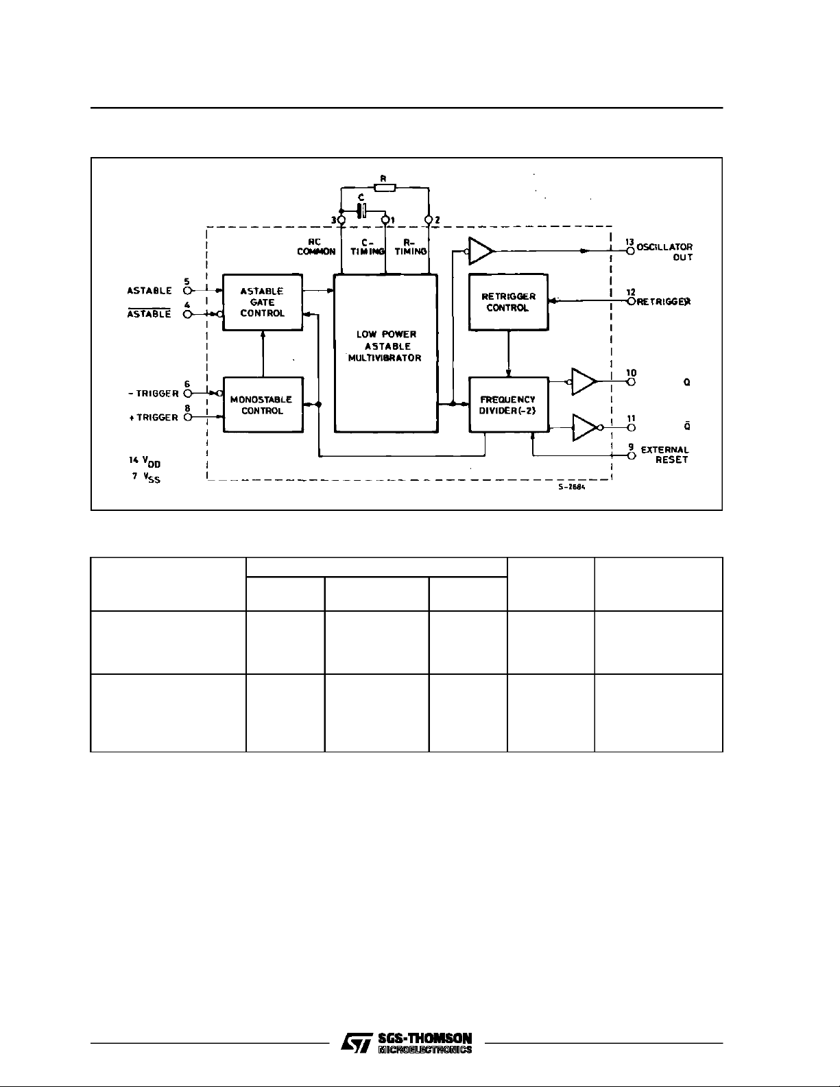
TheHCC4047B (extended temperature range) and
HCF4047B (intermediate temperature range) are
monolithic integrated circuits, available in 14-lead
dual in-line plastic or ceramic package and plastic micropackage. The HCC/HCF4047B consists of
a gatable astablemultivibrator with logictechniques
incorporated to permit positive or negative edgetriggeredmonostablemultivibratoractionwithretriggeringandexternal countingoptions. Inputsinclude
+TRIGGER-TRIGGER,ASTABLE, ASTABLE, RETRIGGER,and EXTERNAL RESET. Buffered outputs are Q, Q, and OSCILLATOR. In all modes of
operation, anexternalcapacitor mustbeconnected
betweenC-TimingandRC-Common terminals, and
an externalresistormust be connectedbetweenthe
R-TimingandRC-Commonterminals.Foroperating
modes see functional terminal connections and application notes.
PIN CONNECTIONS
June1989
1/15
HCC/HCF4047B
BLOCK DI AGRAM
FUNCTIONAL TERMINAL CONNECTIONS
Terminal Connections
Function*
to V
DD
to V
SS
Astable Multivibrator :
Free Running
True Gating
Complement Gating
4, 5, 6, 14
4, 6, 14
6, 14
7, 8, 9, 12
7, 8, 9, 12
5, 7, 8, 9 ,12
Monostable Multivibrator :
Positive–Edge Trigger
Negative–Edge Trigger
Retriggerable
External Countdown**
* In all cases external capacitor and resistor betweenpins, 1, 2 and 3 (see logic diagrams).
** Input pulse to Reset of External Counting Chip.
External Counting Chip Output to pin 4.
4, 14
4, 8, 14
4, 14
14
5, 6, 7, 9, 12
5, 7, 9, 12
5, 6, 7, 9
5, 6, 7, 8, 9, 12
Input
Pulse to
–
5
4
8
6
8, 12
–
Output
Pulse
From
10, 11, 13
10, 11, 13
10, 11, 13
10, 11
10, 11
10, 11
10, 11
Output Period
or
Pulse Width
t
(10, 11) = 4.40RC
A
t
(13) = 2.20RC
A
t
(10, 11) = 2.48RC
M
2/15

HCC/HCF4047B
ABSOLUTE MAXIMUM RATINGS
Symbol Parameter Value Unit
V
* Supply Voltage : HCC Types
DD
HCF Types
V
Input Voltage – 0.5 to VDD+ 0.5 V
i
I
DC Input Current (any one input) ± 10 mA
I
P
Total Power Dissipation (per package)
tot
Dissipation per Output Transistor
for T
= Full Package-temperature Range
op
T
Operating Temperature : HCC Types
op
HCF Types
T
Stresses above those listed under ”Absolute Maximum Ratings” may cause permanent damage to the device. This is a stress
rating only and functional operation of the device at these or any other conditions above those indicated in the operational sections
of this specification is not implied. Exposure to absolute maximum rating conditions for external periods may affect device reliability.
* All voltage values are referred to VSSpin voltage.
Storage Temperature – 65 to + 150 °C
stg
RECOMMENDED OPERATING CONDITIONS
Symbol Parameter Value Unit
V
T
Supply Voltage :HCC Types
DD
HCF Types
V
Input Voltage 0 to V
I
Operating Temperature : HCC Types
op
HCF Types
– 0.5 to + 20
– 0.5 to + 18
200
100
– 55 to + 125
–40to+85
3to18
3to15
DD
– 55 to + 125
–40to+85
V
V
mW
mW
°C
°C
V
V
V
°C
°C
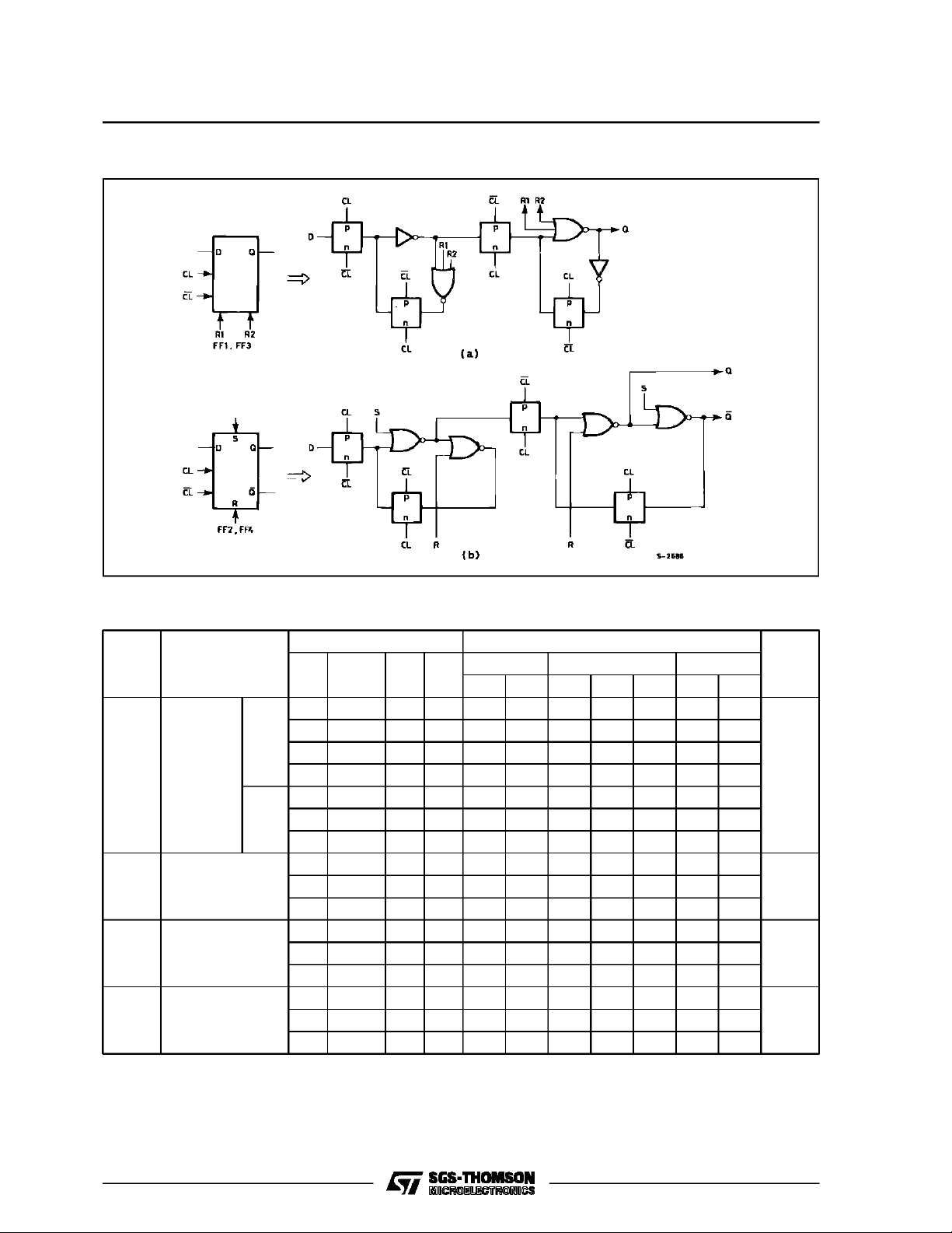
LOGI C DIAGRAM
3/15
HCC/HCF4047B
Detail for Flip-flopsFF1 and FF3(a) and for Flip-flops FF2 and FF4 (b).
STATIC ELECTRICAL CHARACTERISTICS (over recommended operating conditions)
Test Conditions Value
Symbol Parameter
Quiescent
I
L
Current
HCC
Types
HCF
Types
V
OH
Output High
Voltage
V
OL
Output Low
Voltage
V
IH
Input High
Voltage
*T
=–55°CforHCC device : – 40°CforHCF device.
Low
*T
= + 125°CforHCC device : + 85°CforHCF device.
High
The Noise Margin for both ”1” and ”0” level is : 1V min. with VDD= 5V, 2V min. with VDD= 10V, 2.5V min. with VDD= 15V.
V
V
I
(V) (V) (µA) (V)
O
|IO|V
DD
T
* 25°CT
Low
High
*
Min. Max. Min. Typ. Max. Min. Max.
0/ 5 5 1 0.02 1 30
0/10 10 2 0.02 2 60
0/15 15 4 0.02 4 120
0/20 20 20 0.04 20 600
0/ 5 5 4 0.02 4 30
0/10 10 8 0.02 8 60
0/15 15 16 0.02 16 120
0/ 5 < 1 5 4.95 4.95 4.95
0/10 < 1 10 9.95 9.95 9.95
0/15 < 1 15 14.95 14.95 14.95
5/0 < 1 5 0.05 0.05 0.05
10/0 < 1 10 0.05 0.05 0.05
15/0 < 1 15 0.05 0.05 0.05
0.5/4.5 < 1 5 3.5 3.5 3.5
1/9 < 1 10 7 7 7
1.5/13.5 < 1 15 11 11 11
Unit
µA
V
V
V
4/15

HCC/HCF4047B
STATIC ELECTRICAL CHARACTERISTICS (continued)
Test Conditions Value
Symbol Parameter
V
IL
Input Low
Voltage
I
OH
Output
Drive
Current
HCC
Types
HCF
Types
I
OL
Output
Sink
Current
HCC
Types
HCF
Types
I
IH,IIL
Input
leakage
Curent
HCC
Types
HCF
Types
C
Input Capacitance Any Input 5 7.5 pF
I
*T
=–55°C for HCC device : – 40°C for HCF device.
Low
*T
=+125°C for HCC device : + 85°C for HCF device.
High
The Noise Margin for both ”1” and ”0” level is : 1V min. with VDD= 5V, 2V min. with VDD= 10V, 2.5V min. with VDD= 15V.
V
V
I
(V) (V) (µA) (V)
O
|IO|V
DD
T
* 25°CT
Low
Min. Max. Min. Typ. Max. Min. Max.
4.5/0.5 < 1 5 1.5 1.5 1.5
9/1 < 1 10 3 3 3
13.5/1.5 < 1 15 4 4 4
0/ 5 2.5 5 – 2 – 1.6 – 3.2 – 1.15
0/ 5 4.6 5 – 0.64 – 0.51 – 1 – 0.36
0/10 9.5 10 – 1.6 – 1.3 – 2.6 – 0.9
0/15 13.5 15 – 4.2 – 3.4 – 6.8 – 2.4
0/ 5 2.5 5 – 1.53 – 1.36 – 3.2 – 1.1
0/ 5 4.6 5 – 0.52 – 0.44 – 1 – 0.36
0/10 9.5 10 – 1.3 – 1.1 – 2.6 – 0.9
0/15 13.5 15 – 3.6 – 3.0 – 6.8 – 2.4
0/ 5 0.4 5 0.64 0.51 1 0.36
0/10 0.5 10 1.6 1.3 2.6 0.9
0/15 1.5 15 4.2 3.4 6.8 2.4
0/ 5 0.4 5 0.52 0.44 1 0.36
0/10 0.5 10 1.3 1.1 2.6 0.9
0/15 1.5 15 3.6 3.0 6.8 2.4
0/18
18
± 0.1 ±10
–5
± 0.1
Any Input
0/15
15 ± 0.3 ±10
–5
± 0.3 ± 1
High
*
± 1
Unit
V
mA
mA
µA
DYNAMIC ELECTRICAL CHARACTERISTICS (T
=25°C, CL= 50pF, RL= 200kΩ,
amb
typical temperature coefficient for all VDDvalues is 0.3%/°C, all input rise and fall times = 20ns)
Symbol Parameter
t
PLH,tPHL
Propagation
Delay Time
Astable, Astable to
osc. out
Astable, Astable to
Q, Q
+ or – Trigger to
Q, Q
Test Conditions
(V) Min. Typ. Max.
V
DD
5 200 400
10 100 200
15 80 160
5 350 700
10 175 350
15 125 250
5 500 1000
10 225 450
15 150 300
Value
Unit
ns
5/15

HCC/HCF4047B
DYNAMIC ELECTRICAL CHARACTERISTICS (continued)
Symbol Parameter
t
PLH,tPHL
Propagation
Retrigger to Q, Q 5 300 600
Delay Time
External Reset to
Q, Q
t
THL,tTLH
t
w
Transition Time Osc. Out Q, Q 5 100 200
Input Pulse
Width :
t
r,tf
Input Rise and Fall Time All Inputs 5
Q or Q Deviation from 50% Duty
Factor
Test Conditions
(V) Min. Typ. Max.
V
DD
Value
10 150 300
15 100 200
5 250 500
10 100 200
15 70 140
10 50 100
15 40 80
+ Trigger,
– Trigger
5 200 400
10 80 160
15 50 100
Reset 5 100 200
10 50 100
15 30 60
Retrigger 5 300 600
10 115 230
15 75 150
10
Unlimited µs
15
5 ± 0.5 ± 1
10 ± 0.5 ± 1
15 ± 0.1 ± 0.5
Unit
ns
%
Typical Output Low (sink)Current Characteristics.
6/15
Minimum Output Low (sink)Current Characteristics.

HCC/HCF4047B
Typical Output High (source) Current Characteristics.
APPLICATION INFORMATION
1 - CIRCUIT DESCRIPTION
Astableoperation is enabled by a high level on the
ASTABLE input. The periodof thesquare wave at
the Q and Q Outputs in thismode of operation is a
function of the external components employed.
”True” inputpulseson the ASTABLEinputor ”Complement”pulsesontheASTABLEinputallowthe circuit to be used as a gatable multivibrator. The
OSCILLATORoutputperiodwillbehalf of theQterminaloutput in the astable mode. However, a 50%
duty cycle is not guaranteed at this output. In the
monostable mode, positive-edge triggering is accomplished by application of a leading-edge pulse
to the +TRIGGERinput and a low levelto the –TRIGGER input. For negative-edge triggering, a trailing-edge pulse is applied to the –TRIGGER and a
highlevelis applied tothe+TRIGGER.Input pulses
may be of any duration relative to the outputpulse.
The multivibratorcan be retriggered (on the leading
edge only) by applying a common pulse to both the
RETRIGGERand +TRIGGER inputs. In this mode
Minimum Output High (source) Current Characteristics.
the output pulse remains high as long as the input
pulse period is shorter than the period determined
by theRC components. An external countdown option can be implementedby coupling ”Q” to an external”N” counter andresettingthecounter with the
trigger pulse. The counter output pulse is fed back
to the ASTABLE input and has a duration equal to
N times the period of the multivibrator. A high level
on the EXTERNAL RESETinputassures no output
pulse during an ”ON” power condition. This input
can also be activated to terminate the output pulse
at anytime. Inthemonostable mode, a high-level or
power-on reset pulse, must be applied to the EXTERNALRESET whenever VDDis applied.
2 - ASTABLE MODE
The following analysis presents worst-case vari-
ationsfromunit-to-unit asafunctionoftransfer-voltage (VTR) shift (33% – 67% VDD) for free-running
(astable)operation.
7/15

HCC/HCF4047B
ASTABLE MODE WAVEFORMS.
V
t1= – RC In
t2= – RC In
TR
VDD+V
VDD–V
2VDD–V
tA=2(t1+t2)= –2 RC In
TR
TR
TR
(VTR)(VDD–VTR)
(VDD+VTR)(2VDD–VTR)
Typ : VTR=0.5 VDDtA= 4.40 RC
Min : VTR=0.33 VDDtA= 4.62 RC
Max : VTR= 0.67 VDDtA= 4.62 RC
thus if tA=4.40 RC is used, the maximumvari-
ationwill be(+ 5.0%, – 0.0%)
Inaddition tovariations fromunit-to-unit, theastable
MONOSTABLEWAVEFORMS.
Where tM= monostable mode pulse width. Values
for tMareas follows :
Typ : VTR=0.5 VDDtM=2.48 RC
Min : VTR=0.33 VDDtM= 2.71 RC
Max : VTR= 0.67 VDDtM= 2.48 RC
Thus if tM=2.48 RC is used, the maximum vari-
ationwill be(+ 9.3%, – 0.0%).
Note : In the astable mode, the first positive half
cyclehasa duration of TM;succeedingdurations are tA/2.
In addition to variations from unit to unit, the monostable pulse width may vary as a function of frequencywith respect to VDDand temperature.
period may vary as a function of frequency withrespectto VDDandtemperature.
3 - MONOSTABLEMODE
The following analysis presents worst-case vari-
ationsfromunit-to-unit asafunctionoftransfer-voltage (VTR) shift (33% – 67% VDD) for one-shot
(monostable) operation.
V
t1=– RC In
t2=– RC In
tM=(t1+t2)=–RCIn
TR
2V
DD
VDD–V
TR
2VDD–V
TR
(VTR)(VDD–VTR)
(2 VDD–VTR)(2VDD)
modetoextendtheoutput-pulse duration,ortocomparethe frequency of an input signal withthat ofthe
internal oscillator. In the retrigger mode the input
pulseisapplied to terminals8and12,andtheoutput
is taken from terminal 10 or 11. As shown in fig. A
normalmonostable actionis obtainedwhen one retrigger pulse is applied. Extended pulse duration is
obtained when morethan one pulse is applied. For
two input pulses, tRE=t1’+t1+2t2. For more than
two pulses, tRE(Q OUTPUT) terminates at some
variable time tDafter the termination of the last retrigger pulse. tDis variable because tRE(Q OUTPUT) terminates after the second positive edge of
the oscillator output appears at flip-flop 4 (see logic
diagram).
4 - RETRIGGER MODE
The HCC/HCF4047B can be used in the retrigger
8/15

Figure A : Retrigger-mode Waveforms.
HCC/HCF4047B
5 - EXTERNAL COUNTER OPTION
TimetMcanbeextended byanyamountwiththeuse
of external counting circuitry. Advantages include
digitallycontrolledpulseduration,smalltimingcapacitors for long time periods, and extremely fast recoverytime.
Figure B : Implementation of External Counter Option.
6 - POWER CONSUMPTION
In the standby mode (Monostable or Astable),
power dissipation will be a function of leakage current in the circuit, as shown in the static electrical
characteristics. For dynamic operation, the power
needed to charge the external timing capacitor C is
givenby the following formula :
AstableMode : P = 2CV2f. (Outputat Pin 13)
P= 4CV2f. (OutputatPin10and11)
Monostable Mode : P=
(2.9CV2) (Duty Cycle)
T
(Output at Pin 10 and 11)
The circuit is designed so that most of the total
power is consumed in the externalcomponents. In
practice,the lowerthe valuesof frequency and volt-
A typical implementation is shown in fig. B. The
pulseduration at the output is
t
=(N–1)(tA)+(tM+tA/2)
ext
Where t
=pulse duration of the circuitry,and N is
ext
the number ofcounts used.
ageused,theclosertheactualpowerdissipationwill
be to the calculated value.
Becausethe powerdissipationdoes notdepend on
R, adesignforminimum power dissipationwouldbe
a smallvalue of C.The valueofR woulddepend on
the desired period (within the limitations discussed
above).
7 - TIMING-COMPONENTLIMITATIONS
The capacitor used in the circuit shouldbe non-po-
larized andhavelowleakage(i.e.theparallel resistance of the capacitor should be an order of
magnitude greater than the external resistorused).
Threeisnoupper orlowerlimitforeitherRorCvalue
to maintain oscillation.
However, in consideration of accuracy, C must be
much larger than the inherent stray capacitance in
9/15

HCC/HCF4047B
the system (unless this capacitance can be
measured andtakenintoaccount). R must bemuch
largerthan the COS/MOS”ON” resistance inseries
with it,which typically is hundreds of ohms. In addition,with verylarge valuesof R, some short-term instability with respectto time may be noted.
C ≥ 100pF, up to any practical value, for astable
modes;
C ≥ 1000pF, up to any practical value, for monostable modes.
10KΩ ≤ R ≤ 1MΩ.
The recommended values for these componentsto
maintain agreement with previously calculated formulas without trimming should be :
TEST CIRCUITS
QuiescentDevice Current. Input Voltage.
Input Current.
10/15

Plastic DIP14 MECHANICAL DATA
HCC/HCF4047B
DIM.
MIN. TYP. MAX. MIN. TYP. MAX.
a1 0.51 0.020
B 1.39 1.65 0.055 0.065
b 0.5 0.020
b1 0.25 0.010
D 20 0.787
E 8.5 0.335
e 2.54 0.100
e3 15.24 0.600
F 7.1 0.280
I 5.1 0.201
L 3.3 0.130
Z 1.27 2.54 0.050 0.100
mm inch
P001A
11/15

HCC/HCF4047B
Ceramic DIP14/1 MECHANICAL DATA
DIM.
MIN. TYP. MAX. MIN. TYP. MAX.
A 20 0.787
B 7.0 0.276
D 3.3 0.130
E 0.38 0.015
e3 15.24 0.600
F 2.29 2.79 0.090 0.110
G 0.4 0.55 0.016 0.022
H 1.17 1.52 0.046 0.060
L 0.22 0.31 0.009 0.012
M 1.52 2.54 0.060 0.100
N 10.3 0.406
P 7.8 8.05 0.307 0.317
Q 5.08 0.200
mm inch
12/15
P053C

SO14 MECHANICAL DATA
HCC/HCF4047B
DIM.
MIN. TYP. MAX. MIN. TYP. MAX.
A 1.75 0.068
a1 0.1 0.2 0.003 0.007
a2 1.65 0.064
b 0.35 0.46 0.013 0.018
b1 0.19 0.25 0.007 0.010
C 0.5 0.019
c1 45° (typ.)
D 8.55 8.75 0.336 0.344
E 5.8 6.2 0.228 0.244
e 1.27 0.050
e3 7.62 0.300
F 3.8 4.0 0.149 0.157
G 4.6 5.3 0.181 0.208
L 0.5 1.27 0.019 0.050
M 0.68 0.026
S8°(max.)
mm inch
P013G
13/15

HCC/HCF4047B
PLCC20 MECHANICAL DATA
DIM.
MIN. TYP. MAX. MIN. TYP. MAX.
A 9.78 10.03 0.385 0.395
B 8.89 9.04 0.350 0.356
D 4.2 4.57 0.165 0.180
d1 2.54 0.100
d2 0.56 0.022
E 7.37 8.38 0.290 0.330
e 1.27 0.050
e3 5.08 0.200
F 0.38 0.015
G 0.101 0.004
M 1.27 0.050
M1 1.14 0.045
mm inch
14/15
P027A

HCC/HCF4047B
Information furnished is believed to be accurate and reliable. However, SGS-THOMSON Microelectronics assumes no responsability for the
consequences of use of such information nor for any infringement of patents or other rights of third parties which may results from its use. No
license is granted by implication or otherwise underany patent or patent rights of SGS-THOMSON Microelectronics. Specificationsmentioned
in this publication are subject to changewithout notice. This publication supersedes and replaces all information previously supplied.
SGS-THOMSON Microelectronicsproductsare notauthorized for use ascritical componentsinlife supportdevices or systemswithout express
written approval of SGS-THOMSON Microelectonics.
1994 SGS-THOMSON Microelectronics - All Rights Reserved
Australia - Brazil - France - Germany - Hong Kong - Italy - Japan - Korea - Malaysia - Malta - Morocco - The Netherlands -
Singapore - Spain - Sweden - Switzerland - Taiwan - Thailand - UnitedKingdom - U.S.A
SGS-THOMSON Microelectronics GROUP OF COMPANIES
15/15
 Loading...