

QUAD TRUE/COMPLEMENT BUFFER
.BALANCED SINK AND SOURCE CURRENT ;
APPROXIMATELY 4 TIMES STANDARD ”B”
DRIVE
.EQUALIZED DELAY TO TRUE AND COMPLE-
MENT OUTPUTS
.QUIESCENT CURRENT SPECIFIED TO 20V
FOR HCC DEVICE
.5V, 10V AND15V PARAMETRIC RATINGS
.INPUT CURRENTOF100nAAT18VAND 25°C
FOR HCC DEVICE
.100 % TESTEDFOR QUIESCENTCURRENT
.MEETSALLREQUIREMENTSOFJEDECTEN-
TATIVESTANDARDN°13A,”STANDARDSPECIFICATIONS FOR DESCRIPTION OF ”B”
SERIESCMOS DEVICES”
HCC/H CF 4 041 U B
EY
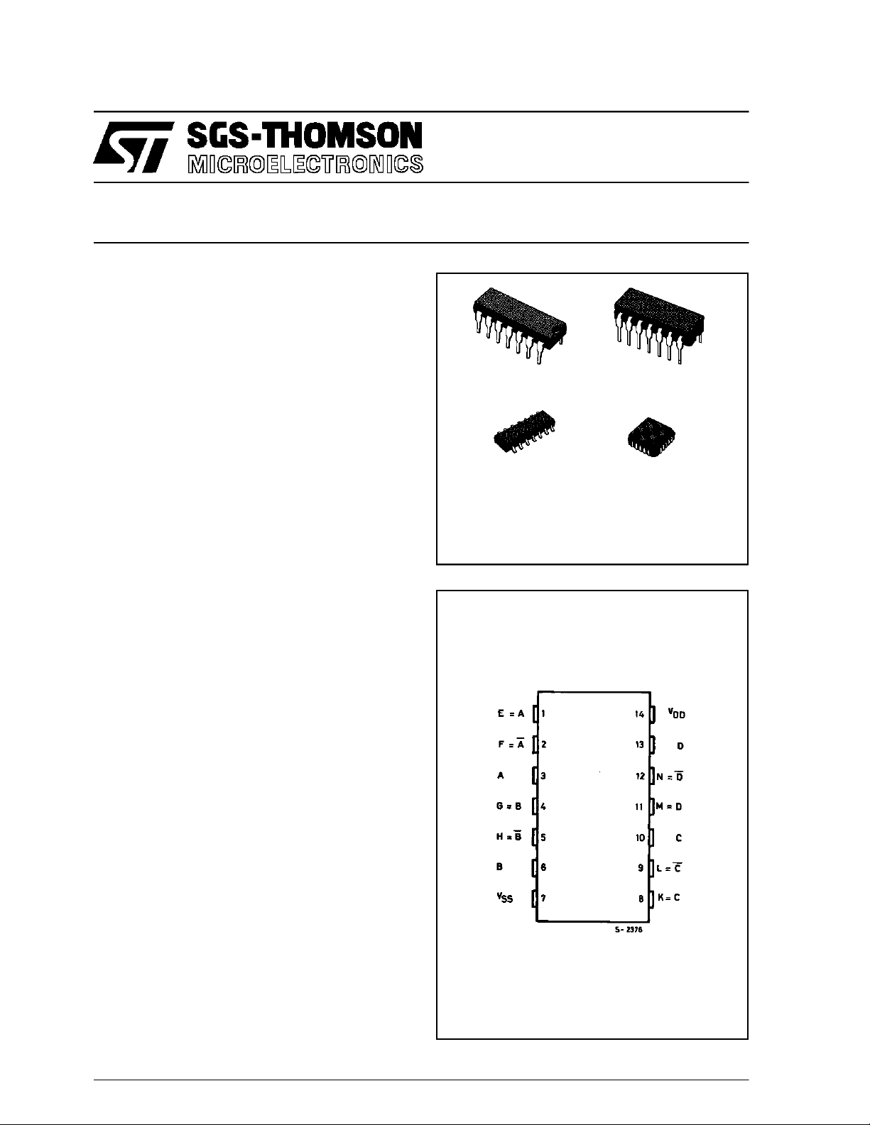
(Plastic Package)F(Ceramic Frit Seal Package)
M1
(MicroPackage)
ORDER CODES :
HCC4041BF HCF4041BM1
HCF4041BEY HCF4041BC1
(PlasticChipCarrier)
C1
DESCRIPTIO N
The HCC4041UB (extended temperature range)
andHCF4041UB(intermediate temperature range)
are monolithic integrated circuits, available in 14lead dual in-line plastic or ceramic package and
plasticmicro package.
TheHCC/HCF4041UB typesarequadtrue/comple-
ment buffers consisting of n- and p-channel units
having low channel resistance and high current
(sourcing and sinking) capability. The HCC/-
HCF4041UB is intended for use as a buffer, line
driver, orCOS/MOS-to-TTLdriver.Itcanbe used as
an ultra-low power resistor-network driver for A/D
and D/A conversion, as a transmission-line driver,
and inother applications where high noiseimmunity
and low-power dissipation are primary design requirements.
PIN C ONN ECT IONS
June1989
1/12
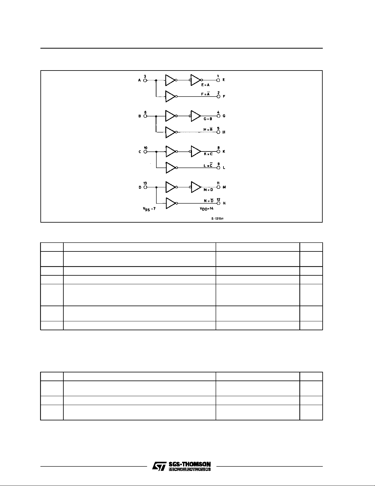
HCC/HCF4041UB
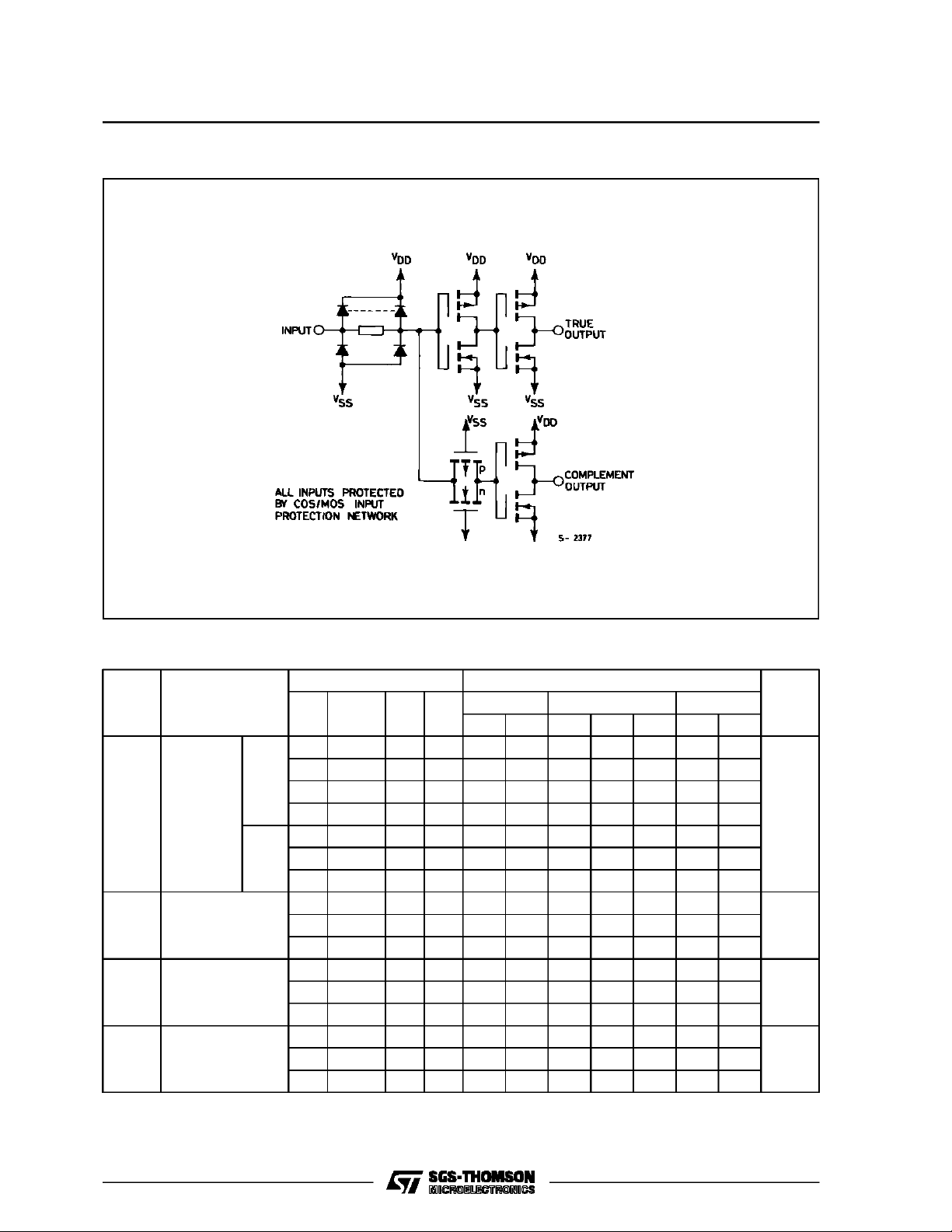
FUN CTIONAL DIAGR A M
ABSOLUTE MAXIMUM RATIN G S
Symbol Parameter Value Unit
V
* Supply Voltage :HC C Types
DD
HCF Types
V
Input Voltage – 0.5 to VDD+ 0.5 V
i
I
DC Input Current (any one input) ± 10 mA
I
P
Total Power Dissipation (per package)
tot
– 0.5 to + 20
– 0.5 to + 18
200
V
V
mW
Dissipation per Output Transistor
for Top= Full Package-temperature Range
T
Operating Temperature :HCC Types
op
HCF Types
T
Stresses above those listed under ”Absolute Maximum Ratings” may cause permanent damage to the device. This is a stress
rating only and functional operation of the device at these or any other conditions above those indicated in the operational sections
of this specification is not implied. Exposure to absolute maximum rating conditions for external periods may affect device reliability.
* All voltage values are referred to VSSpin voltage.
Storage Temperature – 65 to + 150 °C
stg
100
– 55 t o + 125
–40to+85
mW
°C
°C
RECOMMENDED OPERATING CO NDITIONS
Symbol Parameter Value Unit
V
Supply Voltage :HC C Types
DD
HCF Types
V
Input Voltage 0 to V
I
T
Operating Temperature : HCC Types
op
HCF Types
3to+18
3to+15
DD
– 55 t o + 125
–40to+85
V
V
V
°C
°C
2/12
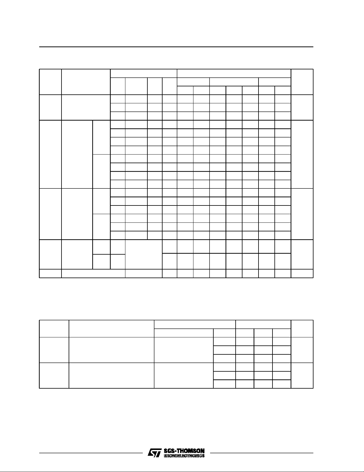
SCHEM ATIC D I A GRA M
HCC/HCF4041UB
STATIC ELECTRICAL CHARACTERISTICS(over recommended operatingconditions)
Test Conditions Valu e
Symbol Parameter
(V) (V) (µA) (V)
I
L
Quiescent
Current
HCC
Types
0/ 5 5 1 0.02 1 30
0/10 10 2 0.02 2 60
0/15 15 4 0.02 4 120
0/20 20 20 0.04 20 600
0/ 5 5 4 0.02 4 30
HCF
Types
0/10 10 8 0.02 8 60
0/15 15 16 0.02 16 120
V
OH
Output High
Voltage
0/ 5 < 1 5 4.95 4.95 4.95
0/10 < 1 10 9.95 9.95 9.95
0/15 < 1 15 14.95 14.95 14.95
V
OL
Output Low
Voltage
5/0 < 1 5 0.05 0.05 0.05
10/0 < 1 10 0.05 0.05 0.05
15/0 < 1 15 0.05 0.05 0.05
V
IH
Input High
Voltage
*T
=–55°CforHCC device : – 40°CforHCF device.
Low
*T
= + 125°CforHCC device : + 85°CforHCF device.
High
The Noise Margin for both ”1” and ”0” level is : 1V min. with VDD= 5V, 2V min. with VDD= 10V, 2.5V min. with VDD= 15V.
V
V
I
O
|IO|V
DD
T
* 25°CT
Low
Min. M ax. Min. Typ. Ma x. Min. Max.
0.5/4.5 < 1 5 4 4 4
1/9 < 1 10 8 8 8
1.5/13.5 < 1 15 12.5 12.5 12.5
High
*
Unit
µA
V
V
V
3/12
HCC/HCF4041UB
STATIC ELECTRICAL CHARACTERISTICS(continued)
Test Conditions Valu e
Symbol Parameter
V
IL
Input Low
Voltage
I
OH
Output
Drive
Current
HCC
Types
HCF
Types
I
OL
Output
Sink
Current
HCC
Types
HCF
Types
I
IH,IIL
Input
leakage
Current
HCC
Types
HCF
Types
C
I
*T
=–55°CforHCC device : – 40°CforHCF device.
Low
*T
High
The Noise Margin for both ”1” and ”0” level is : 1V min. with VDD= 5V, 2V min. with VDD= 10V, 2.5V min. with VDD= 15V.
Input Capacitance Any Input 15 22.5 pF
= + 125°CforHCC device : + 85°CforHCF device.
V
V
O
|IO|V
I
(V) (V) (µA) (V)
T
DD
* 25°CT
Low
Min. M ax. Min. Typ. Ma x. Min. Max.
4.5/0.5 < 1 5 1 1 1
9/1 < 1 10 2 2 2
13.5/1.5 < 1 15 2.5 2.5 2.5
0/ 5 2.5 5 – 8.4 – 6.4 – 12.8 – 4.6
0/ 5 4.6 5 – 2.1 – 1.6 – 3.2 – 1.2
0/10 9.5 10 – 6.25 – 5 – 10 – 3.5
0/15 13.5 15 – 24 – 19 – 38 – 13
0/ 5 2.5 5 – 6.8 – 5.44 – 12.8 – 4.08
0/ 5 4.6 5 – 1.7 – 1.36 – 3.2 – 1.02
0/10 9.5 10 – 5.31 – 4.25 – 10 – 3.18
0/15 13.5 15 –20.18 –16.15 –38 –12.11
0/ 5 0.4 5 2.1 1.6 3.2 1.2
0/10 0.5 10 6.25 5 10 3.5
0/15 1.5 15 24 19 38 13
0/ 5 0.4 5 1.7 1.36 3.2 1.02
0/10 0.5 10 5.31 4.25 10 3.18
0/15 1.5 15 20.18 16.15 38 12.11
–5
0/18
18 ± 0.1 ±10
± 0.1 ± 1
Any Input
0/15
15 ± 0.3 ±10
–5
± 0.3 ± 1
High
*
Unit
V
mA
µA
DYNAMIC ELECTRICAL CHARACTERISTICS (T
=25°C, CL= 50pF, RL= 200kΩ,
amb
typical temperature coefficient for all VDDvalues is 0.3 %/°C,all inputrise and fall times = 20ns)
Symbol Parameter
t
PLH,tPHL
t
THL,tTL H
Propagation Delay Time 5 60 120
Transition Time 5 40 80
4/12
Test Conditions Val ue
V
(V) Min. Typ. Max.
DD
10 35 70
15 25 50
10 20 40
15 15 30
Unit
ns
ns

HCC/HCF4041UB
Minimum Output High (source) Current Characteristics.
Minimum Output Low (sink) Current Characteristics.
TypicalOutput Low(sink) Current.
TypicalOutput High(source) Current Characteristics.
TypicalTransitionTime vs. Load Capacitance. Typical Propagation Delay Timevs. LoadCapacit-
ance.
5/12

HCC/HCF4041UB
Minimum and Maximum Transfer Characteristics-true Output-and Test Circuit.
Minimum MaximumTransfer Characteristics Complement Output-and TestCircuit.
TypicalPower Dissipation vs. Input Rise andFall
Time per Output Pair.
6/12
TypicalPower Dissipationvs. Frequency per Output Pair.

TEST CIRCUI TS
QuiescentDeviceCurrent. Noise Immunity.
Input Leakage Current.
HCC/HCF4041UB
7/12

HCC/HCF4041UB
Plastic DIP14 MECHANICAL DATA
DIM.
MIN. TYP. MAX. MIN. TYP. MAX.
a1 0.51 0.020
B 1.39 1.65 0.055 0.065
b 0.5 0.020
b1 0.25 0.010
D 20 0.787
E 8.5 0.335
e 2.54 0.100
e3 15.24 0.600
F 7.1 0.280
I 5.1 0.201
L 3.3 0.130
Z 1.27 2.54 0.050 0.100
mm inch
8/12
P001A

Ceramic DIP14/1 MECHANICAL DATA
HCC/HCF4041UB
DIM.
MIN. TYP. MAX. MIN. TYP. MAX.
A 20 0.787
B 7.0 0.276
D 3.3 0.130
E 0.38 0.015
e3 15.24 0.600
F 2.29 2.79 0.090 0.110
G 0.4 0.55 0.016 0.022
H 1.17 1.52 0.046 0.060
L 0.22 0.31 0.009 0.012
M 1.52 2.54 0.060 0.100
N 10.3 0.406
P 7.8 8.05 0.307 0.317
Q 5.08 0.200
mm inch
P053C
9/12

HCC/HCF4041UB
SO14 MECHANICAL DATA
DIM.
MIN. TYP. MAX. MIN. TYP. MAX.
A 1.75 0.068
a1 0.1 0.2 0.003 0.007
a2 1.65 0.064
b 0.35 0.46 0.013 0.018
b1 0.19 0.25 0.007 0.010
C 0.5 0.019
c1 45° (typ.)
D 8.55 8.75 0.336 0.344
E 5.8 6.2 0.228 0.244
e 1.27 0.050
e3 7.62 0.300
F 3.8 4.0 0.149 0.157
G 4.6 5.3 0.181 0.208
L 0.5 1.27 0.019 0.050
M 0.68 0.026
S8°(max.)
mm inch
10/12
P013G

PLCC20 MECHANICAL DATA
HCC/HCF4041UB
DIM.
MIN. TYP. MAX. MIN. TYP. MAX.
A 9.78 10.03 0.385 0.395
B 8.89 9.04 0.350 0.356
D 4.2 4.57 0.165 0.180
d1 2.54 0.100
d2 0.56 0.022
E 7.37 8.38 0.290 0.330
e 1.27 0.050
e3 5.08 0.200
F 0.38 0.015
G 0.101 0.004
M 1.27 0.050
M1 1.14 0.045
mm inch
P027A
11/12

HCC/HCF4041UB
Information furnished isbelieved to be accurate and reliable. However, SGS-THOMSON Microelectronicsassumes no responsability forthe
consequences of use of suchinformation norfor any infringementof patents orother rights of third partieswhich may results fromits use. No
license is grantedbyimplication or otherwise underany patent or patentrightsofSGS-THOMSON Microelectronics. Specificationsmentioned
in this publicationare subject to change without notice. This publication supersedes andreplaces all information previously supplied.
SGS-THOMSON Microelectronicsproductsare not authorizedfor use ascritical componentsin life supportdevices or systemswithoutexpress
written approval of SGS-THOMSON Microelectonics.
1994SGS-THOMSON Microelectronics- All RightsReserved
Australia - Brazil - France - Germany - Hong Kong - Italy- Japan - Korea- Malaysia - Malta -Morocco - The Netherlands-
Singapore - Spain - Sweden- Switzerland - Taiwan -Thailand - United Kingdom -U.S.A
SGS-THOMSON Microelectronics GROUP OF COMPANIES
12/12
 Loading...