


DECADECOUNTERS/DIVIDERS WITH DECODED
WITH; DISPLAY ENABLE 4026B
RI PPLE BLANKING 4033B
.COUNTER AND 7-SEGMENT DECODING IN
ONE PACKAGE
.EASILYINTERFACEDWITH 7-SEGMENT DIS-
PLAY TYPES
.FULLY STATIC COUNTER OPERATION : DC
TO 6MHz(typ.) AT VDD= 10V
.IDEAL FOR LOW-POWER DISPLAYS
.DISPLAYENABLE OUTPUT - 4026B
.”RIPPLEBLANKING”ANDLAMP TEST-4033B
.QUIESCENT CURRENT SPECIFIED TO 20V
FOR HCC DEVICE
.STANDARDIZED SYMMETRICAL OUTPUT
CHARACTERISTICS
.5V, 10V,AND 15V PARAMETRIC RATING
.INPUT CURRENTOF100nA AT18V AND25°C
FOR HCC DEVICE
.100% TESTEDFOR QUIESCENTCURRENT
.MEETSALLREQUIREMENTSOFJEDECTEN-
TATIVESTANDARDN°13A,”STANDARDSPECIFICATIONS FOR DESCRIPTION OF ”B”
SERIESCMOS DEVICES”
HCC/H CF4 02 6B
HCC/HCF4033B
7-SEGMENT DISPLAY OUTPUTS
EY
(Plastic Package)
M1
(Micro Package)
ORDER CODES:
HCC40XXBF HCF40XXBM1
HCF40XXBEY HCF40XXBC1
PIN CONN ECT IONS
(CeramicFrit Seal Package)
(Plastic Chip Carrier)
F
C1
DESCRIPTION
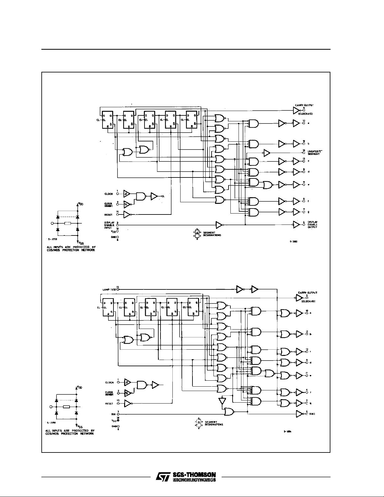
The HCC4026B/4033B (extended temperature
range) and HCF4026B/4033B (intermediate tem-
perature range) are monolithic integrated circuits,
available in 16-lead dual in-line plastic or ceramic
package and plastic micro package. The
HCC/HCF4026B and HCC/HCF4033B each consist of a 5-stage Johnson decade counter and an
outputdecoder which convertsthe Johnsoncodeto
a 7-segment decoded output for driving one stage
in a numerical display. These devices are particularly advantageous in display applications where
lowpower dissipationand/or low packagecount are
important. Inputs common to both types are
CLOCK,RESET,& CLOCKINHIBIT; commonoutputs are CARRYOUT and the seven decoded outputs(a,b,c,d, e, f,g). Additional inputsandoutputs
fortheHCC/HCF4026B include DISPLAY ENABLE
input and DISPLAY ENABLE and UNGATED ”CSEGMENT” outputs. Signals peculiar to the
HCC/HCF4033B are RIPPLE-BLANKING INPUT
AND LAMP TEST INPUT and a RIPPLE-BLANKINGOUTPUT.A high RESET signal clears the de-
June1989
4026B
4033B
1/15

HCC/HCF4026B/4033B
cade counter to its zero count. The counter is advanced one count at the positive clock signal transition if the CLOCK INHIBIT signal is low. Counter
advancement viathe clocklineisinhibited whenthe
CLOCK INHIBIT signal is high. Antilock gating is
provided on the JOHNSON counter, thus assuring
propercounting sequence. The CARRY-OUT(C
out
signal completes one cycle every ten CLOCK
INPUT cycles and isused to clockthe succeeding
decade directly in a multi-decade counting chain.
The sevendecoded outputs (a,b, c,d,e, f, g) illuminate the proper segments in a sevensegment display device used for representing the decimal
numbers 0 to 9. The 7-segment outputs go high on
selection in the HCC/HCF4033B ; in the HCC/-
HCF4026B these outputs go high only when the
DISPLAY ENABLEIN is high.
HCC/HCF4026B- Whenthe DISPLAYENABLE IN
is lowthe seven decoded outputs are forced low regardless of the state of thecounter. Activationof the
display only when required results in significant
power savings. This system also facilitates implementation of display-character multiplexing. The
CARRY OUT and UNGATED ”C-SEGMENT” signals are not gated by the DISPLAY ENABLE and
therefore are availablecontinuously. This feature is
a requirement in implementation of certain divider
functionssuch as divide-by-60 and divide-by-12.
HCC/HCF4033B-TheHCC/HCF4033B has provi-
sions for automatic blanking of the non-significant
zeros in amulti-digit decimal numberwhichresults
in an easily readable display consistent with
normal writing practice. For example, the number
0050.07000 in an eight digit display would be displayed as 50.07. Zero suppression on the integer
side is obtained by connecting the RBI terminal of
the HCC/HCF4033B associated with the most significantdigit in thedisplay to alow-level voltageand
)
connectingtheRBOterminal ofthatstagetotheRBI
terminal of the HCC/HCF4033B in the next-lower
significant position in the display. This procedure is
continued foreach succeedingHCC/HCF4033Bon
the integer side of thedisplay. On thefractionside
of the display the RBIof the HCC/HCF4033B asso-
ciatedwiththe leastsignificant bitis connected to a
low-level voltage and the RBO of that HCC/-
HCF4033B is connected to the RBI terminal of the
HCC/HCF4033B inthenext more-significant-bit po-
sition. Again, this procedure is continued for all
HCC/HCF4033B’s on the fraction side of the display.In a purely fractionalnumberthezero immediately preceding the decimal point can be displayed
by connecting the RBI of that stageto a high level
voltage(instead of tothe RBO of thenextmore-significant-stage). For example : optional zero →
0.7346. Likewise, the zero in a number such as
763.0canbedisplayedbyconnecting the RBI ofthe
HCC/HCF4033B associated with it to a high-level
voltage. Ripple blanking of non-significant zeros
provides an appreciable savings in display power.
The HCC/HCF4033B has a LAMP TEST input
which, when connected to a high-level voltage,
overrides normal decoder operation and enables a
checkto be made on possible displaymalfunctions
by putting the sevenoutputsin thehigh state.
2/15

FUN CTIONAL DIAGR A MS
HCC/HCF4026B/4033B
4026B
4033B
ABSOLUTE MAXIMUM RATINGS
Symbol Parameter Value Unit
* Supply Voltage :HCC Types
V
DD
HCF Types
V
Input Voltage – 0.5 to VDD+ 0.5 V
i
I
DC Input Current (any one input) ± 10 mA
I
P
Total Power Dissipation (per package)
tot
Dissipation per Output Transistor
for T
= Full Package-temperature Range
op
T
Operating Temperature : HCC Types
op
HCF Types
T
Stresses above those listed under ”Absolute Maximum Ratings” may cause permanent damage to the device. This is a stress
rating only and functional operation of the device at these or any other conditions above those indicated in the operational sections of this specification is not implied. Exposure to absolute maximum rating conditions for external periods may affect device
reliability.
*
Allvoltagesvalues are referredto VSSpinvoltage.
Storasge Temperature – 65 to + 150 °C
stg
– 0.5 to + 20
– 0.5 to + 18
200
100
– 55 to + 125
–40to+85
V
V
mW
mW
°C
°C
RECOMMENDED OPERATING CONDITIONS
Symbol Parameter Value Unit
V
T
Supply Voltage : HCC Types
DD
HCF Types
V
Input Voltage 0 to V
I
Operating Temperature : HCC Types
op
HCF Types
3to18
3to15
DD
– 55 to + 125
–40to+85
V
V
V
°C
°C
3/15
HCC/HCF4026B/4033B
LOGIC DIAGRAMS
4026B
4033B
4/15

TIM ING DIAG R AMS
4026B
HCC/HCF4026B/4033B
4033B
5/15

HCC/HCF4026B/4033B
STATIC ELECTRICAL CHARACTERISTICS (overrecommended operating conditions)
Test Conditions Value
Symbol Parameter
Quiescent
I
L
Current
HCC
Types
V
V
O
|IO|V
I
(V) (V) (µA) (V)
DD
T
* 25°CT
Low
High
Min. Max. Min. Typ. Max. Min. Max.
0/ 5 5 5 0.04 5 150
0/10 10 10 0.04 10 300
0/15 15 20 0.04 20 600
0/20 20 100 0.08 100 3000
0/ 5 5 20 0.04 20 150
HCF
Types
0/10 10 40 0.04 40 300
0/15 15 80 0.04 80 600
V
OH
Output High
Voltage
0/ 5 < 1 5 4.95 4.95 4.95
0/10 < 1 10 9.95 9.95 9.95
0/15 < 1 15 14.95 14.95 14.95
V
OL
Output Low
Voltage
5/0 < 1 5 0.05 0.05 0.05
10/0 < 1 10 0.05 0.05 0.05
15/0 < 1 15 0.05 0.05 0.05
V
IH
Input High
Voltage
0.5/4.5 < 1 5 3.5 3.5 3.5
1/9 < 1 10 7 7 7
1.5/13.5 < 1 15 11 11 11
V
IL
Input Low
Voltage
4.5/0.5 < 1 5 1.5 1.5 1.5
9/1 < 1 10 3 3 3
13.5/1.5 < 1 15 4 4 4
I
OH
Output
Drive
Current
HCC
Types
0/ 5 2.5 5 – 2 – 1. 6 – 3.2 –1.15
0/ 5 4.6 5 – 0.64 – 0. 51 – 1 – 0.36
0/10 9.5 10 – 1.6 – 1.3 – 2.6 – 0.9
0/15 13.5 15 – 4.2 – 3. 4 – 6.8 – 2.4
0/ 5 2.5 5 – 1.53 – 1. 36 – 3.2 – 1. 1
HCF
Types
0/ 5 4.6 5 – 0.52 – 0. 44 – 1 – 0.36
0/10 9.5 10 – 1.3 – 1.1 – 2.6 – 0.9
0/15 13.5 15 – 3.6 – 3. 0 – 6.8 – 2.4
I
Output
OL
Sink
Current
HCC
Types
0/ 5 0.4 5 0.64 0.51 1 0.36
0/10 0.5 10 1.6 1.3 2.6 0.9
0/15 1.5 15 4.2 3.4 6.8 2.4
0/ 5 0.4 5 0.52 0.44 1 0.36
HCF
Types
0/10 0.5 10 1.3 1.1 2.6 0.9
0/15 1.5 15 3.6 3.0 6.8 2.4
I
IH,IIL
(*) T
The Noise Margin for both ”1” and ”0” level is : 1V min. with VDD= 5V, 2V min. with VDD= 10V, 2.5V min. with VDD=15V.
Input
Leakage
Current
Input Capacitance Any Input 5 7.5 pF
C
I
=–55°CforHCC device : – 40°CforHCF device.
Low
T
= + 125°C for HCC device : + 85°CforHCF device.
High
HCC
Types
HCF
Types
0/18
0/15
Any Input
18 ± 0.1 ±10
15 ± 0.3 ±10
–5
± 0. 1 ± 1
–5
± 0. 3 ± 1
Unit
*
µA
V
V
V
V
mA
mA
µA
6/15

HCC/HCF4026B/4033B
DYNAMIC ELECTRICAL CHARACTERISTICS (T
=25°C, CL= 50pF, RL= 200kΩ,
amb
typical temperature coefficient for all VDDvalues is 0.3%/°C, all input rise and fall times = 20ns)
Symbol Paramet e r
Test Conditions
(V) Min. Typ. Max.
V
DD
CLOCKED O PERATION
t
PLH,tPHL
Propagation Delay Time
Carry Out Line
5250500
10 100 200
15 75 150
t
PLH,tPHL
Propagation Delay Time
Decode Out Lines
5350700
10 125 250
15 90 180
t
THL,tTLH
Transition Time
Carry Out Line
5100200
10 50 100
15 25 50
f
* Maximum Clock Input Frequency 5 2.5 5
CL
10 5.5 11
15 8 16
t
WC
Clock Pulse Width 5 110 270
10 50 100
15 40 80
t
r,tf
Clock Input Rise or Fall Time 5
10
15
RESET O PERATION
t
, Propagation Delay Time
PLH
Carry Out Line
5275550
10 120 240
15 80 160
t
PLH,tPHL
Propagation Delay Time
Decode Out Lines
5300600
10 125 250
15 90 180
t
WR
Reset Pulse Width 5 100 120
10 50 100
15 25 50
t
rem
Reset Removal Time 5 0 30
10 0 15
15 0 10
* Measured with respect to carry output line.
Value
Unlimited µs
Unit
ns
ns
ns
MHz
ns
ns
ns
ns
ns
7/15

HCC/HCF4026B/4033B
TypicalOutputLow (sink) Current. MinimumOutput Low(sink) CurrentCharacteristics.
Typical Output High (source) Current Characteristics.
Minimum Output High (source) Current Characteristics.
TYPICAL APPLI CA TIONS
Interfacing with Filament Fluorescent Display. Detail ofTypical Flip-flop Stage for Both Types.
8/15

TYPICAL APPLI CA TIONS (continued)
HCC/HCF4026B/4033B
Interfacing with LED Displays (display common
anode).
Interfacing with NIXIE Tube.
(Display Common Cathode).
9/15

HCC/HCF4026B/4033B
Interfacing with LiquidCristal Displays.
TEST CIRCUITS
QuiescentDevice Current.
Input Current.
Input Voltage.
10/15

HCC/HCF4026B/4033B
Plastic DIP16 (0.25) MECHANICAL DATA
DIM.
MIN. TYP. MAX. MIN. TYP. MAX.
a1 0.51 0.020
B 0.77 1.65 0.030 0.065
b 0.5 0.020
b1 0.25 0.010
D 20 0.787
E 8.5 0.335
e 2.54 0.100
e3 17.78 0.700
F 7.1 0.280
I 5.1 0.201
L 3.3 0.130
Z 1.27 0.050
mm inch
P001C
11/15

HCC/HCF4026B/4033B
Ceramic DIP16/1 MECHANICAL DATA
DIM.
MIN. TYP. MAX. MIN. TYP. MAX.
A 20 0.787
B 7 0.276
D 3.3 0.130
E 0.38 0.015
e3 17.78 0.700
F 2.29 2.79 0.090 0.110
G 0.4 0.55 0.016 0.022
H 1.17 1.52 0.046 0.060
L 0.22 0.31 0.009 0.012
M 0.51 1.27 0.020 0.050
N 10.3 0.406
P 7.8 8.05 0.307 0.317
Q 5.08 0.200
mm inch
12/15
P053D

SO16 (Narrow) MECHANICAL DATA
HCC/HCF4026B/4033B
DIM.
MIN. TYP. MAX. MIN. TYP. MAX.
A 1.75 0.068
a1 0.1 0.2 0.004 0.007
a2 1.65 0.064
b 0.35 0.46 0.013 0.018
b1 0.19 0.25 0.007 0.010
C 0.5 0.019
c1 45° (typ.)
D 9.8 10 0.385 0.393
E 5.8 6.2 0.228 0.244
e 1.27 0.050
e3 8.89 0.350
F 3.8 4.0 0.149 0.157
G 4.6 5.3 0.181 0.208
L 0.5 1.27 0.019 0.050
M 0.62 0.024
S8°(max.)
mm inch
P013H
13/15

HCC/HCF4026B/4033B
PLCC20 MECHANICAL DATA
DIM.
MIN. TYP. MAX. MIN. TYP. MAX.
A 9.78 10.03 0.385 0.395
B 8.89 9.04 0.350 0.356
D 4.2 4.57 0.165 0.180
d1 2.54 0.100
d2 0.56 0.022
E 7.37 8.38 0.290 0.330
e 1.27 0.050
e3 5.08 0.200
F 0.38 0.015
G 0.101 0.004
M 1.27 0.050
M1 1.14 0.045
mm inch
14/15
P027A

HCC/HCF4026B/4033B
Information furnished is believed to be accurate and reliable. However, SGS-THOMSON Microelectronicsassumes no responsability for the
consequences of use of such information nor for any infringementofpatents orother rights of third parties which may results from its use. No
license isgranted by implication orotherwise underany patentor patent rights ofSGS-THOMSON Microelectronics. Specificationsmentioned
in this publication are subject to changewithout notice.This publication supersedes andreplaces all information previously supplied.
SGS-THOMSON Microelectronicsproductsare notauthorized foruse ascritical componentsinlife supportdevices orsystemswithout express
written approval of SGS-THOMSON Microelectonics.
1994 SGS-THOMSON Microelectronics - All RightsReserved
Australia - Brazil - France - Germany - Hong Kong - Italy - Japan - Korea - Malaysia - Malta - Morocco - The Netherlands -
Singapore - Spain - Sweden - Switzerland - Taiwan - Thailand - UnitedKingdom - U.S.A
SGS-THOMSON MicroelectronicsGROUP OF COMPANIES
15/15
 Loading...