

.INVERT INPUTS ON ALL ADDERS FOR SUM
COMPLEMENTING APPLICATIONS
.FULLY STATIC OPERATION...DC TO 10MHz
(typ.)@ VDD=10V
.BUFFEREDINPUTS AND OUTPUTS
.SINGLE-PHASE CLOCKING
.STANDARDIZED SYMMETRICAL OUTPUT
CHARACTERISTICS
.QUIESCENT CURRENT SPECIFIED TO 20V
FOR HCC DEVICE
.5V, 10V, AND 15V PARAMETRIC RATING
.INPUT CURRENT OF100nAAT18VAND 25°C
FOR HCC DEVICE
.100% TESTEDFOR QUIESCENTCURRENT
.MEETSALLREQUIREMENTSOFJEDECTEN-
TATIVESTANDARDN°13A,”STANDARDSPECIFICATIONS FOR DESCRIPTION OF ”B”
SERIESCMOS DEVICES”
HCC/HCF4032B
HCC/HCF4038B
TRIPLE SERIAL ADDERS
EY
(Plastic Package)
M1
(MicroPackage)
ORDER CODES :
HCC40XXBF HCF40XXBM1
HCF40XXBEY HCF40XXBC1
(Ceramic Package)
(PlasticChipCarrier)
F
C1
DESCRIPTI ON
The HCC/4032B/4038B (extended temperature
range) and HCF4032B/4038B (intermediate tem-
perature range) are monolithic integrated circuits,
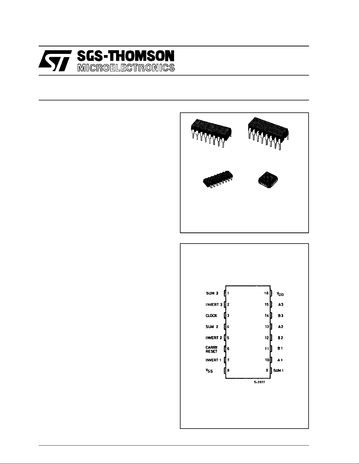
available in 16-lead dual in-line plastic or ceramic
package and plasticmicro package.
The HCC/HCF4032B and HCC/HCF4038B types
consist of three serial adder circuits with common
CLOCK and CARRY-RESET inputs. Each adder
has two provisions for two serial DATA INPUT signals and an INVERT command signal. When the
command signal is a logical ”1”, the sum is complemented. Data words enter the adder with the
leastsignificantbit first;thesignbittrails.Theoutput
istheMOD2sumoftheinput bitsplusthecarry from
the previous bitposition.The carry is only added at
the positive-going clock transition for the
HCC/HCF4032B or at the negative-going clock for
the HCC/HCF4038B, thus, for spike-free operation
the input data transitions should occur as soon as
possible after the triggering edge. The CARRY is
reset to a logical ”0” at the endof each word by applyinga logical ”1” signal toa CARRY-RESET input
one-bit-position before the application of the first bit
of the next word.
PIN CONNECTIONS
June1989
1/11

HCC/HCF4032B/4038B
FUN CTIONAL DIAGR A M
ABSOLUTE M AXI MUM RAT INGS
Symbol Parameter Value Unit
V
* Supply Voltage : HC C Types
DD
HCF Types
V
Input Voltage – 0.5 to VDD+ 0.5 V
i
I
DC Input Current (any one input) ± 10 mA
I
P
Total Power Dissipation (per package)
tot
– 0.5 to + 20
– 0.5 to + 18
200
V
V
mW
Dissipation per Output Transistor
for Top= Full Package-temperature Range
T
Operating Temperature : HCC Types
op
HCF Types
T
Stresses above those listed under ”Absolute Maximum Ratings” may cause permanent damage to the device. This is a stress
rating only and functional operation of the device at these or any other conditions above those indicated in the operational sections
of this specification is not implied. Exposure to absolute maximum rating conditions for external periods may affect device reliability.
* All voltage values are referred to VSSpin voltage.
Storage Temperature – 65 to + 150 °C
stg
100
– 55 to + 125
–40to+85
mW
°C
°C
RECOMMENDED OPERATING CONDITIONS
Symbol Parameter Value Unit
V
T
Supply Voltage : HCC Types
DD
HCF Types
V
Input Voltage 0 to V
I
Operating Temperature : HCC Types
op
HCF Types
3to18
3to15
DD
– 55 to + 125
–40to+85
V
V
V
°C
°C
2/11
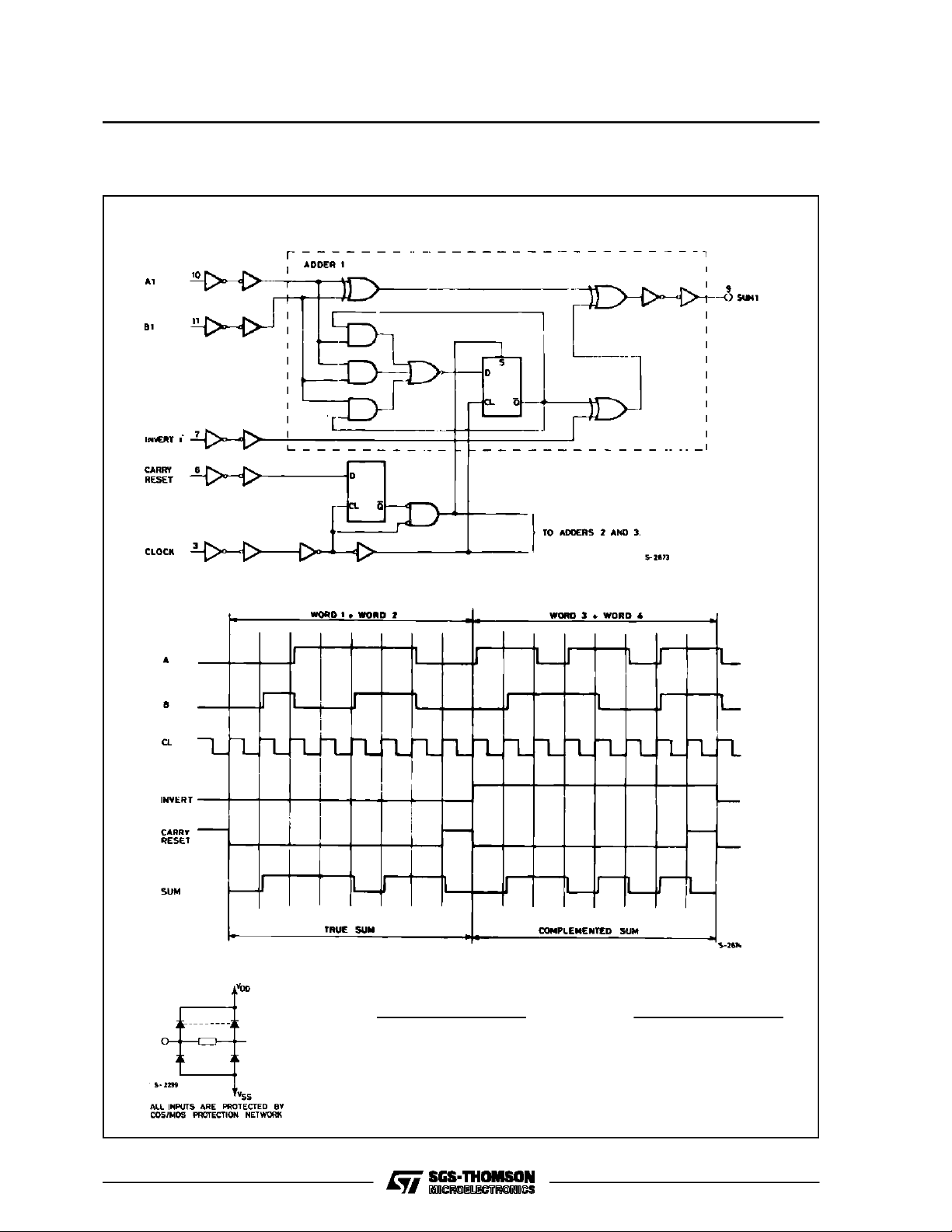
LOGI C AND TIMIN G DIAG RA M S
(oneof three serial adders)
4032B
HCC/HCF4032B/4038B
WORD 1 0.0111100 = + 60
WORD 2 0.0110010 = + 50
0.1101110 = +110
WORD3 1.1011011 = – 37
WORD4 1.1001110 = – 50
1.0101001= –87
3/11
HCC/HCF4032B/4038B
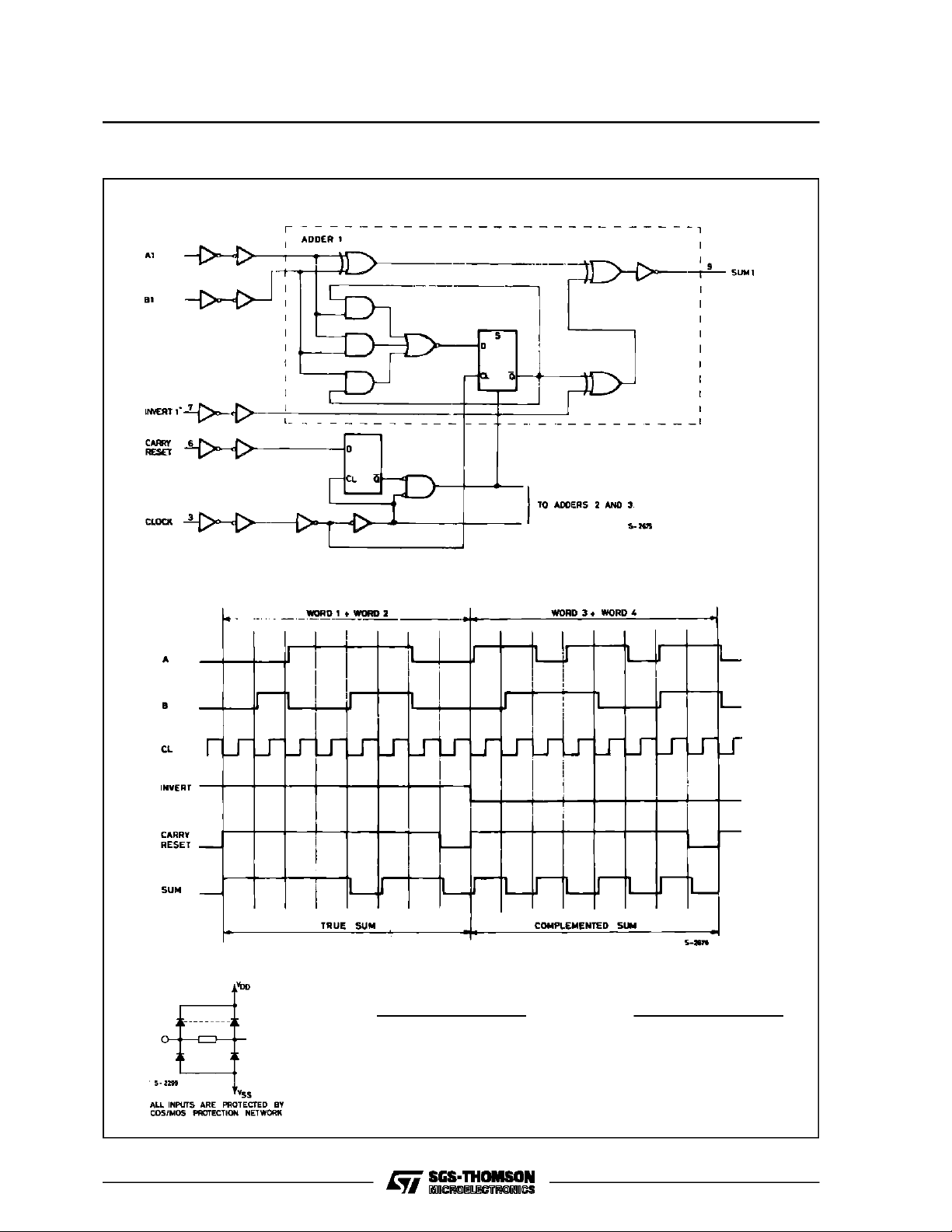
LOGI C AND TIMIN G DIAG RA M S (continued)
4038B
4/11
WORD 1 1.1000011 = – 61
WORD 2 1.1001101 = – 51
1.0010000 = –112
WORD3 0.0100100 = + 36
WORD4 0.0110001 = + 49
0.1010101= + 85
 Loading...