


PRESETTABLE UP/DOWN COUNTER
.MEDIUM SPEED OPERATION - 8MHz (typ.)@
CL= 50pF AND VDD-VSS=10V
.MULTI-PACKAGEPARALLEL CLOCKINGFOR
SYNCHRONOUSHIGH SPEED OUTPUT RESPONSE OR RIPPLE CLOCKING FOR SLOW
CLOCKINPUT RISE AND FALL TIMES
.”PRESET ENABLE” AND INDIVIDUAL ”JAM”
INPUTSPROVIDED
.BINARY OR DECADE UP/DOWNCOUNTING
.BCD OUTPUTSIN DECADEMODE
.STANDARDIZED SYMMETRICAL OUTPUT
CHARACTERISTICS
.5V, 10V, AND 15V PARAMETRIC RATINGS
.INPUT CURRENTOF 100nA AT 18VAND 25°C
FOR HCC DEVICE
.QUIESCENT CURRENT SPECIFIED TO 20V
FOR HCC DEVICE
.100% TESTEDFOR QUIESCENTCURRENT
.MEETSALLREQUIREMENTSOFJEDECTEN-
TATIVE STANDARD No. 13A, ”STANDARD
SPECIFICATIONS FOR DESCRIPTIONOF ”B”
SERIESCMOS DEVICES”
HCC4029B
HCF4029B
BINARY ORBCD DECADE
EY
(PlasticPackage)
M1
(MicroPackage)
ORDER CODES :
HCC4 029BF HCF4029BM1
HCF4029BEY HCF4029BC1
(CeramicPackage)
F
C1
(Chip Carrier)
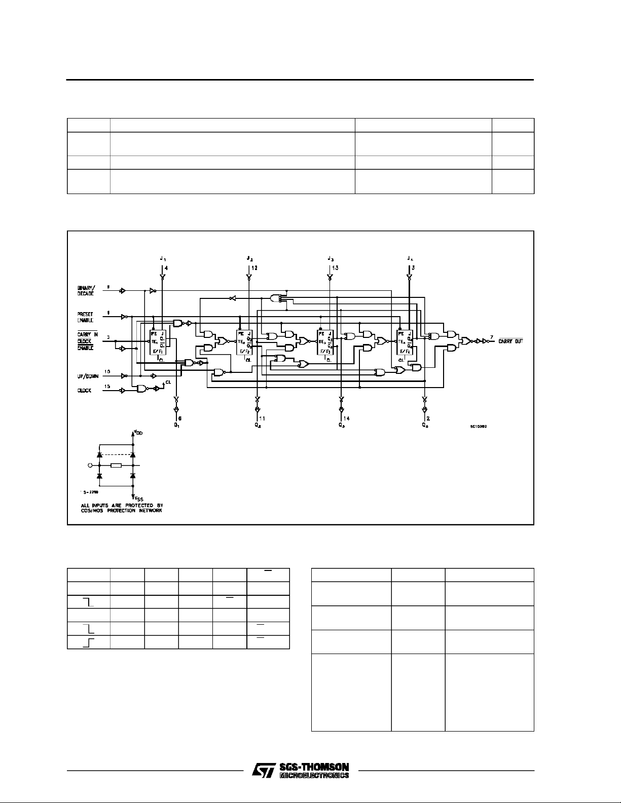
DESCRIPTION
TheHCC4029B (extended temperature range) and
HCF4029B (intermediate temperature range) are
monolithic integrated circuit, available in 16-lead
dual in-line plastic or ceramic package and plastic
micro package.The HCC/HCF4029B consistsof a
four-stage binary or BCD-decade up/downcounter
withprovisions forlook-aheadcarryin bothcounting
modes. The inputs consist of a single CLOCK,
CARRY-IN(CLOCK ENABLE), BINARY/DECADE,
UP/DOWN, PRESET ENABLE, and four individual
JAM signals. Q1, Q2, Q3, Q4 and a CARRY OUT
signalareprovided asoutputs. AhighPRESETENABLEsignal allowsinformationon theJAMINPUTS
to preset the counter to any state asynchronously
with the clock. A low on each JAM line, when the
PRESET-ENABLE signal ishigh,resetsthecounter
toitszerocount. Thecounterisadvancedonecount
at the positive transition of the clock when the
CARRY-INand PRESET ENABLE signals, arelow.
Advancement is inhibited when the CARRY-IN or
PRESET ENABLE signals are high. The CARRYOUT signal is normallyhigh and goes lowwhen the
PIN CONNECTIONS
NC = No Internal Connection
September 1988
1/13

HCC/HCF4029B
counter reachesitsmaximumcount inthe UPmode
or the minimumcountinthe DOWN modeprovided
the CARRY-INsignal is low. The CARRY-IN signal
in the low state can thus be considered a CLOCK
ENABLE. The CARRY-IN terminal must be connectedtoVSSwhennot inuse.Binarycountingisaccomplished when the BINARY/DECADE input is
high ; thecounter counts in thedecade mode when
the BINARY/DECADE input is low. The counter
FUN CTIONAL DI AGR A M
counts Up when to UP/DOWN INPUT is high, and
Down when the UP/DOWN INPUT is low. Multiple
packages can be connected in either a parallelclockingor a ripple-clockingarrangement as shown
in cascading counter packages. Parallel clocking
provides synchronous control and hence faster response from all counting outputs. Ripple-clocking
allowsforlonger clock input rise and fall times.
ABSOLU TE MAXI MU M RAT ING
Symbol Parameter Value Unit
V
* Supply Voltage: HCC Types
DD
V
P
T
T
Stressesabove those listedunder”AbsoluteMaximum Ratings”maycausepermanent damagetothedevice.Thisisastressratingonlyand functional
operation of the device at these or any otherconditions above thoseindicated in theoperational sections of thisspecificationisnotimplied.Exposure
to absolute maximum ratingconditionsforexternal periods mayaffect device reliability.
Allvoltage values are referredtoVSSpinvoltage.
Input Voltage -0.5 to VDD+ 0.5 V
i
DC Input Current (any one input) ± 10 mA
I
I
Total Power Dissipation (per package)
tot
Dissipation per Output Transistor
for Top = Full Package Temperature Range
Operating Temperature: HCC Types
op
Storage Temperature -65 to +150
stg
HCF Types
HCF Types
-0.5 to +20
-0.5 to +18
200
100
-55 to +125
-40 to +85
V
V
mW
mW
o
C
o
C
o
C
2/13
HCC/HCF4029B
RECO MM ENDED OPERAT IN G C ONDITIO NS
Symbol Parameter Value Unit
V
V
T
LOGIC DI AGRAMS
Supply Voltage: HCC Types
DD
HCF Types
Input Voltage 0 to V
I
Operating Temperature: HCC Types
op
HCF Types
3to18
3to15
DD
-55 to +125
-40 to +85
V
V
V
o
C
o
C
TRUTH TABLES
CLOCK TE PE J Q Q
XXOOOI
OIXQ Q
XXOIIO
IIXQQNC
XIXQQNC
X DON’TCARE
Control Input Logic Level Action
BIN/DEC
(B/D)
UP/DOWN
(U/D)
Preset Enable
(PE)
I
O
I
O
I
O
Binary Count
Decade Count
Up Count
Down Count
Jam In
No Jam
No Counter
I
Carry In (Cl)
Advance at Pos.
Clock Transition
(Clock Enable)
Advance Counter
O
at Pos. Clock
Transition
3/13
HCC/HCF4029B
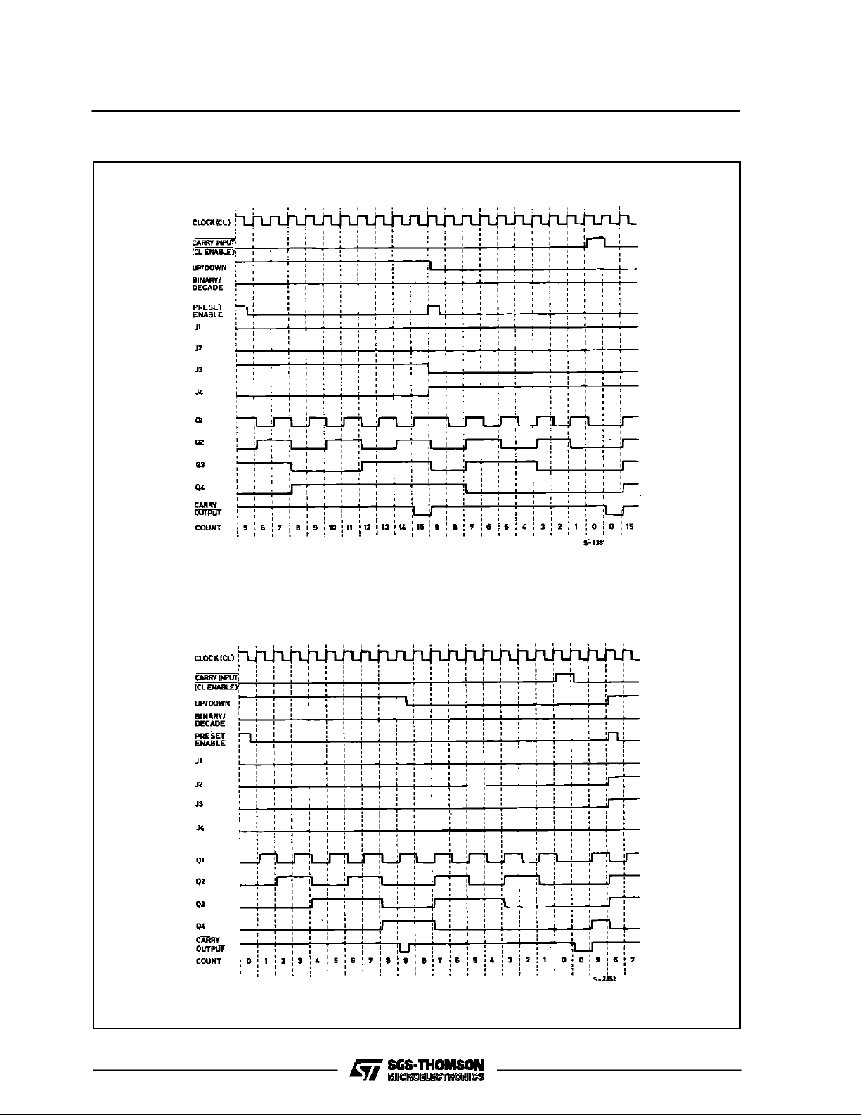
TIM ING DIAGRAMS
Binary Mode
Decade Mode
4/13

HCC/HCF4029B
STATI C ELECT RIC AL CHA R ACTE R ISTI CS (over rec ommended o p er ating conditio ns)
Test Conditios Value
Symbol Parameter
Quiescent
I
L
Current
HCC
Types
V
(V)
V
I
(V)
|IO|
(µA)
V
(V)
O
T
DD
*25
LOW
Min. Max. Min. Typ. Max. Min. Max.
0/5 5 5 0.04 5 150
0/10 10 10 0.04 10 300
0/15 15 20 0.04 20 600
o
CT
0/20 20 100 0.08 100 3000
HCF
Types
0/5 5 20 0.04 20 150
0/10 10 40 0.04 40 300
0/15 15 80 0.04 80 600
OH
Output High
V
Voltage
0/5 < 1 5 4.95 4.95 4.95
0/10 < 1 10 9.95 9.95 9.95
0/15 < 1 15 14.95 14.95 14.95
OL
Output Low
V
Voltage
5/0 < 1 5 0.05 0.05 0.05
10/0 < 1 10 0.05 0.05 0.05
15/0 < 1 15 0.05 0.05 0.05
IH
Input High
V
Voltage
0.5/4.5 < 1 5 3.5 3.5 3.5
1/9 < 1 10 7 7 7
1.5/13.5 < 1 15 11 11 11
IL
Input Low
V
Voltage
4.5/0.5 < 1 5 1.5 1.5 1.5
9/1 < 1 10 3 3 3
13.5/1.5 < 1 15 4 4 4
OH
Output
Drive
Current
HCC
Types
I
0/5 2.5 5 -2 -1.6 -3.2 -1.15
0/5 4.6 5 -0.64 -0.51 -1 -0.36
0/10 9.5 10 -1.6 -1.3 -2.6 -0.9
0/15 13.5 15 -4.2 -3.4 -6.8 -2.4
0/5 2.5 5 -1.53 -1.36 -3.2 -1.1
HCF
Types
0/5 4.6 5 -0.52 -0.44 -1 -0.36
0/10 9.5 10 -1.3 -1.1 -2.6 -0.9
0/15 13.5 15 -3.6 -3.0 -6.8 -2.4
I
OL
Output
Sink
Current
HCC
Types
HCF
Types
0/5 0.4 5 0.64 0.51 1 0.36
0/10 0.5 10 1.6 1.3 2.6 0.9
0/15 1.5 15 4.2 3.4 6.8 2.4
0/5 0.4 5 0.52 0.44 1 0.36
0/10 0.5 10 1.3 1.1 2.6 0.9
0/15 1.5 15 3.6 3.0 6.8 2.4
I
IH,IIL
Input
Leakage
Current
C
*T
LOW
*T
HIGH
TheNoiseMarginfor both ”1” and”0”level is: 1V min. withVDD=5V,2 V min.withVDD=10V,2.5 V min. withVDD=15V
Input Capacitance Any Input 5 7.5 pF
I
=-55oCforHCC device: -40oC for HCF device.
=+125oCforHCC device:+85oC for HCF device.
HCC
Types
HCF
Types
0/18
18 ±0.1 ±10
Any Input
0/15 15 ±0.3 ±10
-5
±0.1 ±1
-5
±0.3 ±1
HIGH
Unit
*
µA
V
V
V
V
mA
mA
µA
5/13

HCC/HCF4029B
DYNAMIC ELECTRICAL CHARACTERISTICS (T
=25oC, CL=50pF,RL= 200 KΩ,
amb
typic al t emper at ure coeff ic ent for al l VDDvalues is 03 %/oC, all input rise and f al l times = 20 ns )
Symbol Parameter
t
t
t
t
t
t
t
r,tf
t
setup
t
setup
f
PLH
PHL
PLH
PHL
TLH
THL
t
max
Propagation Delay Time (Q Outputs) 5 250 500
Propagation Delay Time (Carry Output) 5 280 560
Transition Time (Q Outputs, Carry Output) 5 100 200
Minimum Clock Pulse Width 5 90 180
W
** Clock Rise and Fall Time 5 15
* Minimum Setup Time (Carry Input) 5 30 60
Minimum Setup Time (B/D or UD) 5 170 340
Maximum Clock Input Frequency 5 2 4
PRESET ENABLE
Propagation Delay Time (Q Outputs) 5 235 470
Propagation Delay Time (Carry Output) 5 320 640
Minimum Preset Enable (Pulse Width) 5 65 130
W
* Minimum Preset Enable (Removal Time) 5 100 200
t
t
t
t
t
rem
PLH
PHL
PLH
PHL
t
CARRY INPUT
t
PHL
t
PLH
t
setup
t
hold
* FromUp/Down, Binary/Decade, Carry In orPreset Enable ControlInputs toClock Edge
** If more than oneunit is cascated in theparallel clocked application tr should be made less than or equalto the sumof the fixed propagation
delayat 15pF and the transition time of the carry output drivingstageforthe estimated capacitance load.
*** FromCarryin toClockEdge.
Propagation Delay Time (Carry Output) 5 170 340
*** Minimum Setup Time (Carry In) 5 25 50
Minimum Hold Time (Carry In) 5 100 200
Test Conditions Value
V
(V) Min. Typ. Max.
DD
10 120 240
15 90 180
10 130 260
15 95 190
10 50 100
15 40 80
10 45 90
15 30 60
10 15
15 15
10 10 20
15 6 12
10 70 140
15 50 100
10 4 8
15 5.5 11
10 100 200
15 80 160
10 145 290
15 105 210
10 35 70
15 25 50
10 55 110
15 40 80
10 70 140
15 50 100
10 15 30
15 12 25
10 35 70
15 30 60
Unit
ns
ns
ns
ns
µs
ns
MHz
ns
ns
ns
ns
ns
6/13

HCC/HCF4029B
TypicalOutput Low (sink)Current Characteristics. MinimumOutput Low(sink) Current Charac-
TypicalOutput High (source) Current Characteristics.
Minimum Output High (source) Current Characteristics.
7/13

HCC/HCF4029B
APPLICATIONS
Conversion of Clockup, ClockDown Input Signals to Clock and Up/DownInputsSignals.
Cascading Counter Packages.
The HCC/HCF4029B CLOCK and UP/DOWN in-
puts are useddirectly in mostapplications. In applications where CLOCK UP and CLOCK DOWN
inputs are provided, conversion to the
HCC/HCF4029B CLOCK and UP/DOWN inputs
can easily be realized by use of the circuit.
HCC/HCF4029Bchanges count on positivetransitions of CLOCK UP or CLOCK DOWN inputs. For
the gate configuration shown below, whencounting
up the CLOCK DOWN input must be maintained
high and conversely when counting down the
CLOCKUP inputmust bemaintained high.
* CARRY-OUT lines at the 2nd, 3rd, et., stages may have a negative-going glitch pulse resulting from differential delays of different
HCC/HCF4029B IC’s.Thesenegative-going glitchesdo notaffect proper HCC/HCF4029B operation. However, if the CARRY-OUTsignals
are usedtotriggerotheredge-sensitive logicdevices, such as FF’sorcounters, the CARRY-OUTsignalsshouldbe gatedwiththe clocksignal
usinga 2-input NOR gate suchas HCC/HCF4001B.
RippleClockingMode : The Up/Downcontrolcan be changed at any count. Theonly restrictionon changing the Up/Down control is thatthe
clock inputto thefirstcounting stage must be high.
8/13

Plastic DIP16 (0.25) MECHANICAL DATA
HCC/HCF4029B
DIM.
MIN. TYP. MAX. MIN. TYP. MAX.
a1 0.51 0.020
B 0.77 1.65 0.030 0.065
b 0.5 0.020
b1 0.25 0.010
D 20 0.787
E 8.5 0.335
e 2.54 0.100
e3 17.78 0.700
F 7.1 0.280
I 5.1 0.201
L 3.3 0.130
Z 1.27 0.050
mm inch
P001C
9/13

HCC/HCF4029B
Ceramic DIP16/1 MECHANICAL DATA
DIM.
MIN. TYP. MAX. MIN. TYP. MAX.
A 20 0.787
B 7 0.276
D 3.3 0.130
E 0.38 0.015
e3 17.78 0.700
F 2.29 2.79 0.090 0.110
G 0.4 0.55 0.016 0.022
H 1.17 1.52 0.046 0.060
L 0.22 0.31 0.009 0.012
M 0.51 1.27 0.020 0.050
N 10.3 0.406
P 7.8 8.05 0.307 0.317
Q 5.08 0.200
mm inch
10/13
P053D

SO16 (Narrow) MECHANICAL DATA
HCC/HCF4029B
DIM.
MIN. TYP. MAX. MIN. TYP. MAX.
A 1.75 0.068
a1 0.1 0.2 0.004 0.007
a2 1.65 0.064
b 0.35 0.46 0.013 0.018
b1 0.19 0.25 0.007 0.010
C 0.5 0.019
c1 45° (typ.)
D 9.8 10 0.385 0.393
E 5.8 6.2 0.228 0.244
e 1.27 0.050
e3 8.89 0.350
F 3.8 4.0 0.149 0.157
G 4.6 5.3 0.181 0.208
L 0.5 1.27 0.019 0.050
M 0.62 0.024
S8°(max.)
mm inch
P013H
11/13

HCC/HCF4029B
PLCC20 MECHANICAL DATA
DIM.
MIN. TYP. MAX. MIN. TYP. MAX.
A 9.78 10.03 0.385 0.395
B 8.89 9.04 0.350 0.356
D 4.2 4.57 0.165 0.180
d1 2.54 0.100
d2 0.56 0.022
E 7.37 8.38 0.290 0.330
e 1.27 0.050
e3 5.08 0.200
F 0.38 0.015
G 0.101 0.004
M 1.27 0.050
M1 1.14 0.045
mm inch
12/13
P027A

HCC/HCF4029B
Information furnished is believed to be accurate and reliable. However, SGS-THOMSON Microelectronics assumes no responsability forthe
consequences of use of such information nor for any infringement of patents or other rights of third parties which may results from its use. No
license is granted byimplication orotherwise underany patentor patentrights of SGS-THOMSON Microelectronics.Specificationsmentioned
in this publication aresubject to changewithout notice. Thispublication supersedes and replaces all information previously supplied.
SGS-THOMSON Microelectronicsproducts are not authorized foruse ascritical componentsinlifesupportdevices orsystemswithoutexpress
written approval of SGS-THOMSON Microelectonics.
1994 SGS-THOMSON Microelectronics- All RightsReserved
Australia - Brazil - France - Germany - Hong Kong - Italy - Japan - Korea - Malaysia - Malta - Morocco - The Netherlands-
Singapore -Spain - Sweden - Switzerland - Taiwan - Thailand - UnitedKingdom - U.S.A
SGS-THOMSON Microelectronics GROUP OF COMPANIES
13/13
 Loading...