

.BCD-TO-DECIMAL DECODING OR BINARY-
TO-OCTALDECODING
.HIGHDECODEDOUTPUTDRIVECAPABILITY
.”POSITIVE LOGIC” INPUTS AND OUTPUTS :
DECODED OUTPUTS GO HIGH ON SELECTION
.MEDIUM-SPEED OPERATION : t
80ns (typ.) @ VDD=10V
PHL,tPLH
.STANDARDIZED SYMMETRICAL OUTPUT
CHARACTERISTICS
.QUIESCENT CURRENT SPECIFIED TO 20V
FOR HCC DEVICE
.5V, 10V,AND 15V PARAMETRIC RATINGS
.INPUT CURRENTOF100nA AT18V AND25°C
FOR HCC DEVICE
.100% TESTEDFOR QUIESCENTCURRENT
.MEETSALLREQUIREMENTSOFJEDECTEN-
TATIVESTANDARDN°13A,”STANDARDSPECIFICATIONS FOR DESCRIPTION OF ”B”
SERIESCMOS DEVICES”
HCC/HCF4028B
BCD-TO-DECIMAL DECODER
=
EY
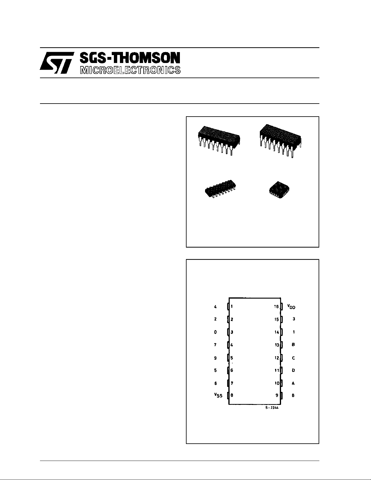
(Plastic Package)
M1
(MicroPackage)
HCC4028BF HCF4028BM1
HCF4028BEY HCF4028BC1
(CeramicFrit SealPackage)
ORDERCODES :
F
C1
(Plastic Chip Carrier)
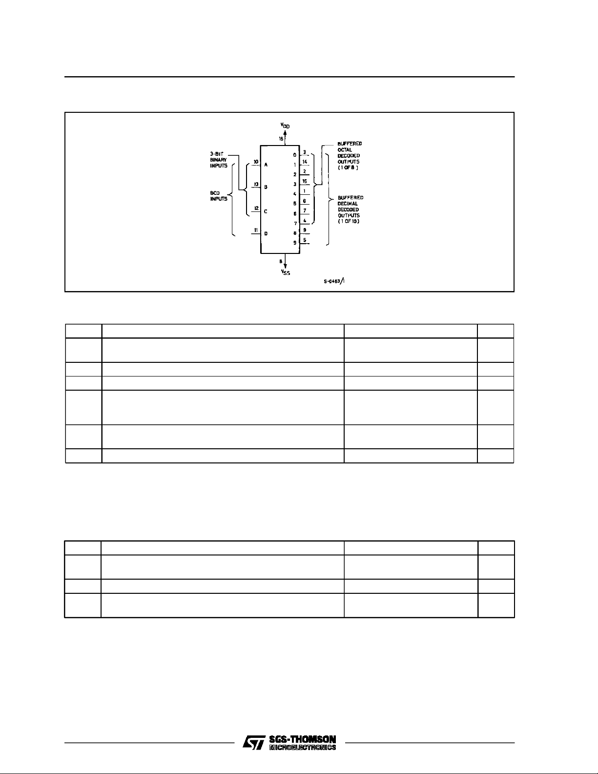
DESCRIPTION
TheHCC4028B(extended temperature range) and
HCF4028B (intermediate temperature range) are
monolithic integrated circuit, available in 16-lead
dual in-line plastic or ceramic package and plastic
micropackage.
The HCC/HCF4028B typesare BCD-to-decimal or
binary-to-octal decoders consisting of buffering on
all4inputs,decoding-logic gates,and10outputbuffers. A BCD code applied to thefourinputs, A to D,
resultsin a high level at the selected one of 10 decimaldecodedoutputs.Similarly,a3-bit binary code
applied to inputs A through C is decoded in octal
codeat output0 to 7ifD =”0”. Highdrive capability
isprovided atalloutputstoenhancedcand dynamic
performance inhigh fan-out applications.
PIN CON NECTIONS
June1989
1/14
HCC/HCF4028B
FUNCTIONAL DIAGRAM
ABSOLUTE MAXIMUM RA TING S
Symbol Parameter Valu e Unit
V
* Supply Voltage : HCC Types
DD
HCF Types
V
Input Voltage – 0.5 to VDD+ 0.5 V
i
DC Input Current (any one input) ± 10 mA
I
I
P
Total Power Dissipation (per package)
tot
Dissipation per Output Transistor
for Top= Full Package-temperature Range
T
Operating Temperature : HCC Types
op
HCF Types
T
Stresses above those listed under ”Absolute Maximum Ratings” may cause permanent damage to the device. This is a stress
rating only and functional operation of the device at these or any other conditions above those indicated in the operational sections of this specification is not implied. Exposure to absolute maximum rating conditions for external periods may affect device
reliability.
* All voltage values are referred to VSSpin voltage.
Storage Temperature – 65 to + 150 °C
stg
– 0.5 to + 20
– 0.5 to + 18
200
100
–55to+125
–40to+85
V
V
mW
mW
°C
°C
RECOMMENDED OPERATING CONDITIONS
Symbol Parameter Value Unit
V
T
2/14
Supply Voltage : HCC Types
DD
HCF Types
V
Input Voltage 0 to V
I
Operating Temperature : HCC Types
op
HCF Types
3to18
3to15
DD
– 55 to + 125
–40to+85
V
V
V
°C
°C
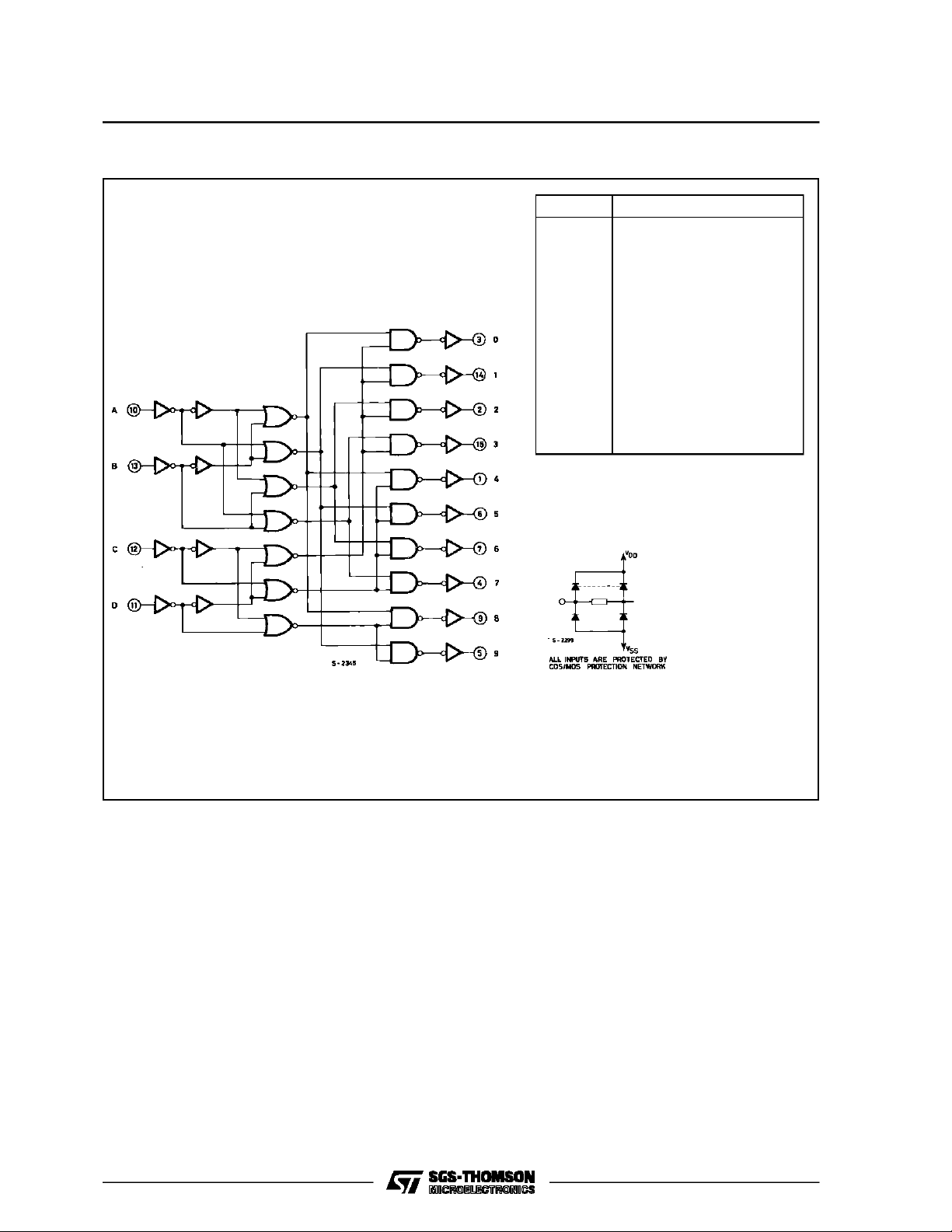
LOGIC DIAGRAM AND TRUTH TABLE
HCC/HCF4028B
DCBA0123456789
0
0
0
0
1
0
0
0
0
0
0
0
0
0
0
1
0
1
0
0
0
0
0
0
0
1
1
1
1
1
1
1
1
0
0
1
1
1
1
0
0
0
0
1
1
1
1
1
1
0
0
1
1
0
0
1
1
0
0
1
1
0
1
0
1
0
1
0
1
0
1
0
1
0
1
0
0
0
0
0
0
0
0
0
0
0
0
0
0
0
0
0
0
0
0
0
0
0
0
0
0
0
0
1
0
0
0
0
0
0
0
0
0
0
0
0
0
0
0
1
0
0
0
0
0
0
0
0
0
0
0
0
WHERE 1 = HIGH LEVEL
0 = LOW LEVEL
0
0
0
1
0
0
0
0
0
0
0
0
0
0
0
0
0
0
0
1
0
0
0
0
0
0
0
0
0
0
0
0
0
0
0
1
0
0
0
0
0
0
0
0
0
0
0
0
0
0
0
1
0
0
0
0
0
0
0
0
0
0
0
0
0
0
0
0
1
0
0
0
0
0
0
0
0
0
0
0
0
0
0
0
0
1
0
0
0
0
0
0
3/14
HCC/HCF4028B
STATIC ELECTRICAL CHARACTERISTICS (over recommended operatingconditions)
Test Conditions Valu e
Symbol Parameter
I
Quiescent
L
Current
HCC
Types
HCF
Types
V
OH
Output High
Voltage
V
OL
Output Low
Voltage
V
IH
Input High
Voltage
V
IL
Input Low
Voltage
I
OH
Output
Drive
Current
HCC
Types
HCF
Types
I
OL
Output
Sink
Current
HCC
Types
HCF
Types
I
IH,IIL
Input
Leakage
Current
HCC
Types
HCF
Types
Input Capacitance Any Input 5 7.5 pF
C
I
*T
=–55°CforHCC device : – 40°CforHCF device.
Low
*T
= + 125°CforHCC device : + 85°CforHCF device.
High
TheNoiseMarginfor both ”1” and ”0” levelis:1V min.with VDD=5V,2V min. withVDD= 10V,2.5V min.with VDD= 15V.
V
V
O
|IO|V
I
(V) (V) (µA) (V)
T
DD
* 25°CT
Low
Min. Max. Min. Typ. Max. Min. Max.
High
0/ 5 5 5 0.04 5 150
0/10 10 10 0.04 10 300
0/15 15 20 0.04 20 600
0/20 20 100 0.08 100 3000
0/ 5 5 20 0.04 20 150
0/10 10 40 0.04 40 300
0/15 15 80 0.04 80 600
0/ 5 < 1 5 4.95 4.95 4.95
0/10 < 1 10 9.95 9.95 9.95
0/15 < 1 15 14.95 14.95 14.95
5/0 < 1 5 0.05 0.05 0.05
10/0 < 1 10 0.05 0.05 0.05
15/0 < 1 15 0.05 0.05 0.05
0.5/4.5 < 1 5 3.5 3.5 3.5
1/9 < 1 10 7 7 7
1.5/13.5 < 1 15 11 11 11
4.5/0.5 < 1 5 1.5 1.5 1.5
9/1 < 1 10 3 3 3
13.5/1.5 < 1 15 4 4 4
0/5 2.5 5 – 2 – 1.6 – 3.2 – 1.15
0/5 4.6 5 – 0.64 – 0.51 – 1 – 0.36
0/10 9.5 10 – 1.6 – 1.3 – 2.6 – 0.9
0/15 13.5 15 – 4.2 – 3.4 – 6.8 – 2.4
0/5 2.5 5 – 1.53 – 1.36 – 3.2 – 1.1
0/5 4.6 5 – 0.52 – 0.44 – 1 – 0.36
0/10 9.5 10 – 1.3 – 1.1 – 2.6 – 0.9
0/15 13.5 15 – 3.6 – 3.0 – 6.8 – 2.4
0/5 0.4 5 0.64 0.51 1 0.36
0/10 0.5 10 1.6 1.3 2.6 0.9
0/15 1.5 15 4.2 3.4 6.8 2.4
0/5 0.4 5 0.52 0.44 1 0.36
0/10 0.5 10 1.3 1.1 2.6 0.9
0/15 1.5 15 3.6 3.0 6.8 2.4
0/18
18 ± 0.1 ±10
–5
± 0.1 ± 1
Any Input
0/15
15 ± 0.3 ±10
–5
± 0.3 ± 1
Unit
*
µA
V
V
V
V
mA
mA
µA
4/14
HCC/HCF4028B
DYNAMIC ELECTRICAL CHARACTERISTICS (T
=25°C, CL= 50pF, RL= 200kΩ,
amb
typical temperature coefficient forall VDDvalues is 0.3%/°C, all input rise and fall times = 20ns)
Symbol Paramet e r
t
PHL,tPLH
t
THL,tTLH
Propagation Delay Time
(clock to ”out”)
Transition Time 5 100 200
Minimum Output High (source) Current Charac-
Test Conditions
V
(V) Min. Typ. M ax.
DD
5175350
10 80 160
15 60 120
10 50 100
15 40 80
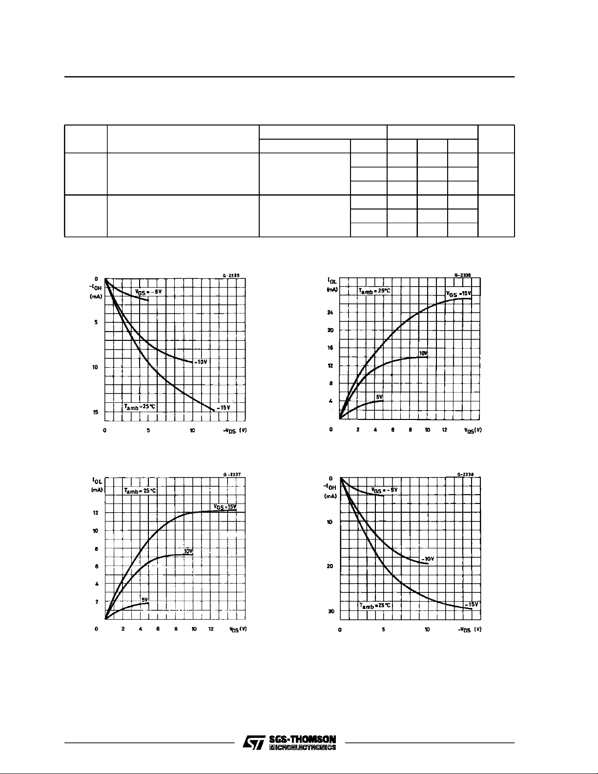
TypicalOutput Low (sink) Current.
Value
teristics.
Unit
ns
ns
Minimum Output Low (Sink) Current Characteristics.
Typical Output High (source) Current Characteristics.
5/14

HCC/HCF4028B
TypicalPropagation Delay Time as aFunction load
Capacitance.
TYPICAL APPLICATIONS
The circuitshown infig.1convertsany 4-bitcodeto
a decimalor hexadecimal codeFig 2 showsanumberof codes and thedecimalor hexadecimal number in these codes which must be applied to the
inputpinsoftheHCC/HCF4028B toselecta particu-
TypicalDynamicPowerDissipation asa Function of
Input Frequency .
lar output. For example : inorder togeta ”high” on
output n8 the input must be either an 8 expressed
in 4-bit binary code, a 15 expressed in 4-bit gray
code, or a 5expressed in excess-3code.
Figure 1 : Code Conversion Circuit.
6/14

Figure 2 : Code Conversion Chart.
HCC/HCF4028B
7/14

HCC/HCF4028B
TYPICAL APPLICATIONS (continued)
Figure 3 : 6-bit binaryto 1 of 64 Adress Decoder.
Figure 4 : Neon Readout (nixie tube)Display
Application.
8/14

TEST CIRCUITS
HCC/HCF4028B
QuiescentDeviceCurrent.
Input Leakage Current.
Noise Immunity.
Dynamic Power Dissipation.
TypicalTransition Timevs. Load Capacitance.
9/14

HCC/HCF4028B
Plastic DIP16 (0.25) MECHANICAL DATA
DIM.
MIN. TYP. MAX. MIN. TYP. MAX.
a1 0.51 0.020
B 0.77 1.65 0.030 0.065
b 0.5 0.020
b1 0.25 0.010
D 20 0.787
E 8.5 0.335
e 2.54 0.100
e3 17.78 0.700
F 7.1 0.280
I 5.1 0.201
L 3.3 0.130
Z 1.27 0.050
mm inch
10/14
P001C

Ceramic DIP16/1 MECHANICAL DATA
HCC/HCF4028B
DIM.
MIN. TYP. MAX. MIN. TYP. MAX.
A 20 0.787
B 7 0.276
D 3.3 0.130
E 0.38 0.015
e3 17.78 0.700
F 2.29 2.79 0.090 0.110
G 0.4 0.55 0.016 0.022
H 1.17 1.52 0.046 0.060
L 0.22 0.31 0.009 0.012
M 0.51 1.27 0.020 0.050
N 10.3 0.406
P 7.8 8.05 0.307 0.317
Q 5.08 0.200
mm inch
P053D
11/14

HCC/HCF4028B
SO16 (Narrow) MECHANICAL DATA
DIM.
MIN. TYP. MAX. MIN. TYP. MAX.
A 1.75 0.068
a1 0.1 0.2 0.004 0.007
a2 1.65 0.064
b 0.35 0.46 0.013 0.018
b1 0.19 0.25 0.007 0.010
C 0.5 0.019
c1 45° (typ.)
D 9.8 10 0.385 0.393
E 5.8 6.2 0.228 0.244
e 1.27 0.050
e3 8.89 0.350
F 3.8 4.0 0.149 0.157
G 4.6 5.3 0.181 0.208
L 0.5 1.27 0.019 0.050
M 0.62 0.024
S8°(max.)
mm inch
12/14
P013H

PLCC20 MECHANICAL DATA
HCC/HCF4028B
DIM.
MIN. TYP. MAX. MIN. TYP. MAX.
A 9.78 10.03 0.385 0.395
B 8.89 9.04 0.350 0.356
D 4.2 4.57 0.165 0.180
d1 2.54 0.100
d2 0.56 0.022
E 7.37 8.38 0.290 0.330
e 1.27 0.050
e3 5.08 0.200
F 0.38 0.015
G 0.101 0.004
M 1.27 0.050
M1 1.14 0.045
mm inch
P027A
13/14

HCC/HCF4028B
Information furnished is believed tobe accurateand reliable.However, SGS-THOMSON Microelectronics assumes no responsability forthe
consequences of use of such information nor for any infringementofpatents orother rights of third parties which may results from its use. No
license isgrantedby implication or otherwiseunder any patent orpatentrights of SGS-THOMSONMicroelectronics.Specificationsmentioned
in this publication are subject to changewithout notice. This publication supersedes and replaces all information previously supplied.
SGS-THOMSON Microelectronicsproductsare notauthorizedforuseascritical componentsin life supportdevices orsystemswithout express
written approval of SGS-THOMSON Microelectonics.
1994 SGS-THOMSON Microelectronics - All RightsReserved
Australia - Brazil - France - Germany- HongKong -Italy-Japan- Korea - Malaysia - Malta - Morocco - The Netherlands-
Singapore - Spain - Sweden - Switzerland - Taiwan - Thailand - UnitedKingdom - U.S.A
SGS-THOMSON MicroelectronicsGROUPOF COMPANIES
14/14
 Loading...