

HCC/HCF4000B-4001B
HCC/HCF4002B-4025B
NOR GATE
4000B–DUAL 3 INPUTPLUS INVERTER
4001B–QUAD 2 INPUT
4002B-DUAL 4 INPUT
4025B TRIPLE3 INPUT
.PROPAGATIONDELAY TIME = 60 ns(typ.) AT
CL= 50 pF,VDD=10V
.BUFFERED INPUTS AND OUTPUTS
.STANDARDIZED SYMMETRICAL OUTPUT
CHARACTERISTICS
.QUIESCENT CURRENT SPECIFIED TO 20 V
FOR HCC DEVICE
.5V, 10V AND 15VPARAMETRIC RATINGS
.INPUT CURRENTOF 100nAAT18VAND25
FOR HCC DEVICE
o
C
.100% TESTED FOR QUIESCENTCURRENT
.MEETSALLREQUIREMENTSOFJEDECTEN-
TATIVE STANDARD N. 13A, ” STANDARD
SPECIFICATIONS FOR DESCRIPTION OF B
SERIESCMOS DEVICES ”
DESCRIPTION
The HCC4000B, HCC4001B, HCC4002B and
HCC4025B (extended temperature range) and
HCF4000B, HCF4001B, HCF4002B and
HCF4025B (intermediate temperature range) are
monolithic integrated circuit, available in 14-lead
dual in line plastic or ceramicpackage and plastic
micropackage.
The HCC/HCF4000B, HCC/HCF4001B,HCC/HCF
4002B and HCC/HCF4025B nor gate provide the
system designer with direct implementation of the
nor function and supplement the existing family of
COS/MOS gates. All inputs and outputs are buffered.
EY
(PlasticPackage)
M1
(MicroPackage)
ORDER CODES :
HCCXXX XBF HCFXXXXBM1
HCFXXXXBEY HCFXXXXBC1
(CeramicPackage)
F
C1
(Chip Carrier)
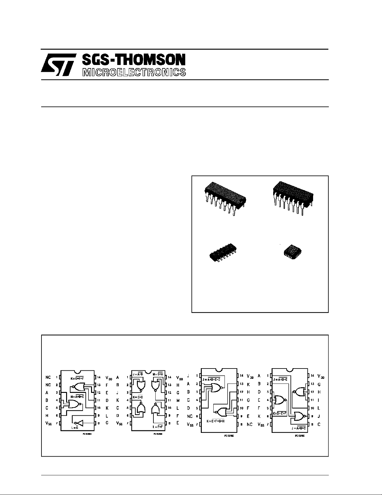
PIN CONNECTIONS
4000 B 4002 B4001 B 4025 B
September 1988
1/13

HCC/H CF4000B-4001B-4002B-4025B
ABSOLU TE MAXIMU M RAT ING
Symbol Parameter Value Unit
V
* Supply Voltage: HCC Types
DD
HCF Types
V
P
Input Voltage -0.5 to VDD+ 0.5 V
i
I
DC Input Current (any one input) ± 10 mA
I
Total Power Dissipation (per package)
tot
Dissipation per Output Transistor
for Top = Full Package Temperature Range
T
Operating Temperature: HCC Types
op
HCF Types
T
Stressesabove thoselistedunder”AbsoluteMaximumRatings”maycause permanent damagetothedevice.Thisisastressratingonlyand functional
operation of the device atthese or any otherconditionsabove thoseindicatedin theoperationalsections of thisspecification is not implied.Exposure
to absolute maximum ratingconditions forexternal periods may affect device reliability.
* All voltagevalues are referred to VSSpinvoltage.
Storage Temperature -65 to +150
stg
RECO MM ENDED OPERATIN G C O NDITI ONS
Symbol Parameter Value Unit
V
V
T
Supply Voltage: HCC Types
DD
HCF Types
Input Voltage 0 to V
I
Operating Temperature: HCC Types
op
HCF Types
-0.5 to +20
-0.5 to +18
200
100
-55 to +125
-40 to +85
3to18
3to15
DD
-55 to +125
-40 to +85
V
V
mW
mW
o
C
o
C
o
C
V
V
V
o
C
o
C
2/13
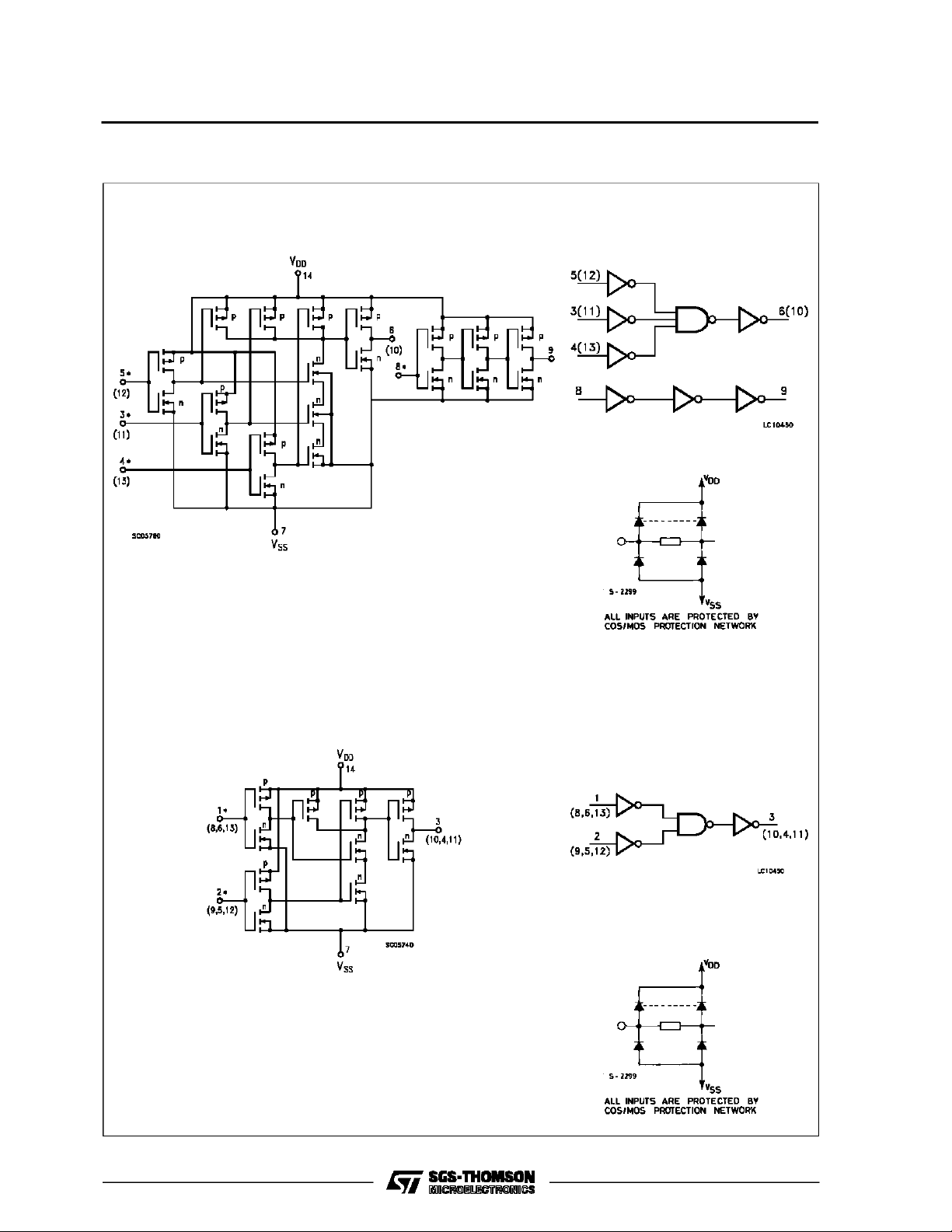
SCHEM ATIC A ND LO GIC D I AG R AMS
HCC/ HCF4000B-4001B-4002B-4025B
4000B
INVERTERAND 1OF 2GATES(NUMBERS INPARANTHESESARE
THERMINALFOR SECONDGATE)
4001B
1 OF 4 GATES (NUMBERS IN PARANTHESES ARE THERMINAL FOR
OTHERGATE)
3/13
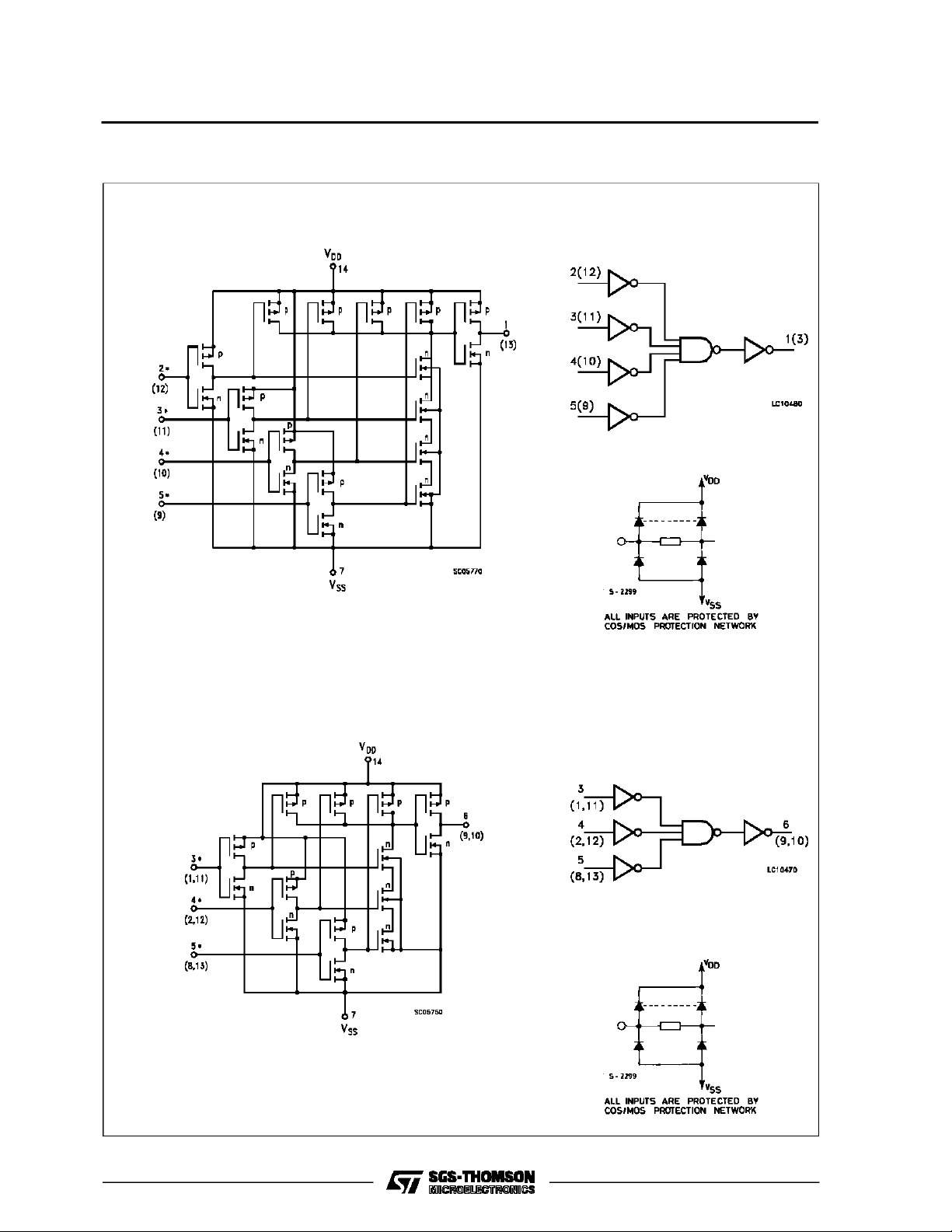
HCC/H CF4000B-4001B-4002B-4025B
SCHEM ATIC A ND LO GIC D I AG R AMS (cont inued)
4002B
1 OF2 GATES(NUMBERSIN PARANTHESESARETHERMINALFOR SECOND GATE)
4025B
INVERTERAND 1OF 3GATES(NUMBERS INPARANTHESESARE
THERMINALFOR OTHERGATES)
4/13

HCC/ HCF4000B-4001B-4002B-4025B
STATI C ELECT RIC AL CHAR ACTER I STI CS (ov er recommend ed op erating co ndi tions )
Test Conditios Value
Symbol Parameter
I
Quiescent
L
Current
HCC
Types
V
(V)
V
I
(V)
|IO|
(µA)
V
(V)
O
T
DD
*25
LOW
Min. Max. Min. Typ. Max. Min. Max.
0/5 5 0.25 0.01 0.25 7.5
0/10 10 0.5 0.01 0.5 15
0/15 15 1 0.01 1 30
o
CT
0/20 20 5 0.02 5 150
HCF
Types
0/5 5 1 0.01 1 7.5
0/10 10 2 0.01 2 15
0/15 15 4 0.01 4 30
OH
Output High
V
Voltage
0/5 < 1 5 4.95 4.95 4.95
0/10 < 1 10 9.95 9.95 9.95
0/15 < 1 15 14.95 14.95 14.95
V
OL
Output Low
Voltage
5/0 < 1 5 0.05 0.05 0.05
10/0 < 1 10 0.05 0.05 0.05
15/0 < 1 15 0.05 0.05 0.05
V
IH
Input High
Voltage
0.5/4.5 < 1 5 3.5 3.5 3.5
1/9 < 1 10 7 7 7
1.5/13.5 < 1 15 11 11 11
V
IL
Input Low
Voltage
4.5/0.5 < 1 5 1.5 1.5 1.5
9/1 < 1 10 3 3 3
13.5/1.5 < 1 15 4 4 4
I
OH
Output
Drive
Current
HCC
Types
0/5 2.5 5 -2 -1.6 -3.2 -1.15
0/5 4.6 5 -0.64 -0.51 -1 -0.36
0/10 9.5 10 -1.6 -1.3 -2.6 -0.9
0/15 13.5 15 -4.2 -3.4 -6.8 -2.4
0/5 2.5 5 -1.53 -1.36 -3.2 -1.1
HCF
Types
0/5 4.6 5 -0.52 -0.44 -1 -0.36
0/10 9.5 10 -1.3 -1.1 -2.6 -0.9
0/15 13.5 15 -3.6 -3.0 -6.8 -2.4
I
OL
Output
Sink
Current
HCC
Types
HCF
Types
0/5 0.4 5 0.64 0.51 1 0.36
0/10 0.5 10 1.6 1.3 2.6 0.9
0/15 1.5 15 4.2 3.4 6.8 2.4
0/5 0.4 5 0.52 0.44 1 0.36
0/10 0.5 10 1.3 1.1 2.6 0.9
0/15 1.5 15 3.6 3.0 6.8 2.4
I
IH,IIL
C
I
Input
Leakage
Current
Input
HCC
Types
HCF
Types
0/18
18 ±0.1 ±10
Any Input
0/15 15 ±0.3 ±10
Any Input 5 7.5
-5
±0.1 ±1
-5
±0.3 ±1
Capacitance
*T
=-55oCforHCC device:-40oC for HCF device.
LOW
*T
=+125oCforHCC device: +85oC for HCF device.
HIGH
TheNoiseMargin for both ”1” and ”0” level is: 1V min. withVDD=5V, 2V min.withVDD=10 V,2.5 V min.withVDD=15V
HIGH
Unit
*
µA
V
V
V
V
mA
mA
µA
pF
5/13

HCC/H CF4000B-4001B-4002B-4025B
DYNAMIC ELECTRICAL CHARACTERISTICS (T
=25oC, CL=50pF,RL= 200 KΩ,
amb
typic al temper at ure coefficent for all VDDvalues is 03 %/oC, all input ris e and fal l times= 20 ns)
Symbol Parameter
t
PHL
t
PLH
t
THL
t
TLH
Propagation Delay Time 5 125 250
Transition Time 5 100 200
Test Conditions Value
(V) Min. Typ. Max.
V
DD
10 60 120
54590
10 50 100
15 40 80
Unit
ns
ns
Typical Output Low (sink) Current Characteristics Minimum Output Low (sink) Current Charac-
teristics
Typical Output High (source) Current Characteristics
6/13
Minimum Output High (sorce) Current Characteristics

HCC/ HCF4000B-4001B-4002B-4025B
Typical Transition Time vs Load Capacitance
Typical Voltage Transfer Characteristics as a
Function of Temperature
Typical Propagation Delay Time vs Load Capacitance
Typical Power Dissipation Per Gate vs Frequency
7/13

HCC/H CF4000B-4001B-4002B-4025B
TEST CIRCUITS
QuiescentDevice Current. Noise Immunity.
Input Leakage Current.
8/13

HCC/ HCF4000B-4001B-4002B-4025B
Plastic DIP14 MECHANICAL DATA
DIM.
MIN. TYP. MAX. MIN. TYP. MAX.
a1 0.51 0.020
B 1.39 1.65 0.055 0.065
b 0.5 0.020
b1 0.25 0.010
D 20 0.787
E 8.5 0.335
e 2.54 0.100
e3 15.24 0.600
F 7.1 0.280
I 5.1 0.201
L 3.3 0.130
Z 1.27 2.54 0.050 0.100
mm inch
P001A
9/13

HCC/H CF4000B-4001B-4002B-4025B
Ceramic DIP14/1 MECHANICAL DATA
DIM.
MIN. TYP. MAX. MIN. TYP. MAX.
A 20 0.787
B 7.0 0.276
D 3.3 0.130
E 0.38 0.015
e3 15.24 0.600
F 2.29 2.79 0.090 0.110
G 0.4 0.55 0.016 0.022
H 1.17 1.52 0.046 0.060
L 0.22 0.31 0.009 0.012
M 1.52 2.54 0.060 0.100
N 10.3 0.406
P 7.8 8.05 0.307 0.317
Q 5.08 0.200
mm inch
10/13
P053C

HCC/ HCF4000B-4001B-4002B-4025B
SO14 MECHANICAL DATA
DIM.
MIN. TYP. MAX. MIN. TYP. MAX.
A 1.75 0.068
a1 0.1 0.2 0.003 0.007
a2 1.65 0.064
b 0.35 0.46 0.013 0.018
b1 0.19 0.25 0.007 0.010
C 0.5 0.019
c1 45° (typ.)
D 8.55 8.75 0.336 0.344
E 5.8 6.2 0.228 0.244
e 1.27 0.050
e3 7.62 0.300
F 3.8 4.0 0.149 0.157
G 4.6 5.3 0.181 0.208
L 0.5 1.27 0.019 0.050
M 0.68 0.026
S8°(max.)
mm inch
P013G
11/13

HCC/H CF4000B-4001B-4002B-4025B
PLCC20 MECHANICAL DATA
DIM.
MIN. TYP. MAX. MIN. TYP. MAX.
A 9.78 10.03 0.385 0.395
B 8.89 9.04 0.350 0.356
D 4.2 4.57 0.165 0.180
d1 2.54 0.100
d2 0.56 0.022
E 7.37 8.38 0.290 0.330
e 1.27 0.050
e3 5.08 0.200
F 0.38 0.015
G 0.101 0.004
M 1.27 0.050
M1 1.14 0.045
mm inch
12/13
P027A

HCC/ HCF4000B-4001B-4002B-4025B
Information furnished is believed to be accurate and reliable.However, SGS-THOMSON Microelectronicsassumes no responsability forthe
consequences of useof such information norfor any infringement of patents or other rights of third partieswhich mayresults from its use. No
license is granted byimplication orotherwiseunderany patent orpatent rights ofSGS-THOMSON Microelectronics. Specificationsmentioned
in this publication are subject to change without notice. This publication supersedes andreplaces all information previously supplied.
SGS-THOMSON Microelectronicsproducts are not authorized foruse ascritical componentsinlife support devices or systems without express
written approval of SGS-THOMSON Microelectonics.
1994 SGS-THOMSON Microelectronics- All Rights Reserved
Australia - Brazil - France - Germany - HongKong - Italy - Japan - Korea - Malaysia- Malta - Morocco - The Netherlands -
Singapore -Spain - Sweden- Switzerland - Taiwan - Thailand - UnitedKingdom - U.S.A
SGS-THOMSON Microelectronics GROUP OF COMPANIES
13/13
 Loading...