

HCC/H CF4 02 57B
QUAD 2-LINE-TO-1-LINE DATA SELECTOR/MULTIPLEXER
.3-STATE OUTPUTS
.STANDARDIZED SYMMETRICAL OUTPUT
CHARACTERISTICS
.5V, 10V,AND 15V PARAMETRIC RATINGS
.INPUT CURRENTOF100nA AT18V AND 25°C
FOR HCC DEVICE
.100% TESTEDFOR QUIESCENTCURRENT
.MEETSALLREQUIREMENTSOF JEDECTEN-
TATIVESTANDARDN°13A,”STANDARDSPECIFICATIONS FOR DESCRIPTION OF ”B”
SERIESCMOS DEVICES”
EY
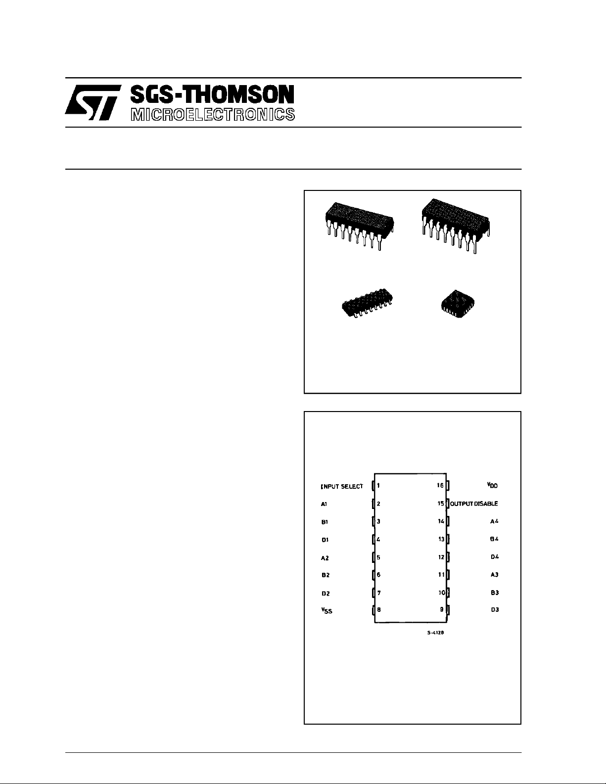
(Plastic Package)F(Ceramic Frit Seal Package)
DESCRIPTION
The HCC40257B (extended temperature range)
and HCF40257B (intermediate temperature range)
are monolithic integrated circuits, available in 16lead dual in-line plastic or ceramic package and
plasticmicro package.
The HCC/HCF40257B is a Data Selector/Multi-
plexerfeaturingthree-state outputs whichcaninterfacedirectlywithanddrivedatalinesofbus-oriented
systems.
M1
(MicroPackage)
ORDER CODES :
HCC40257BF HCF40257BM1
HCF40257BEY HCF40257BC1
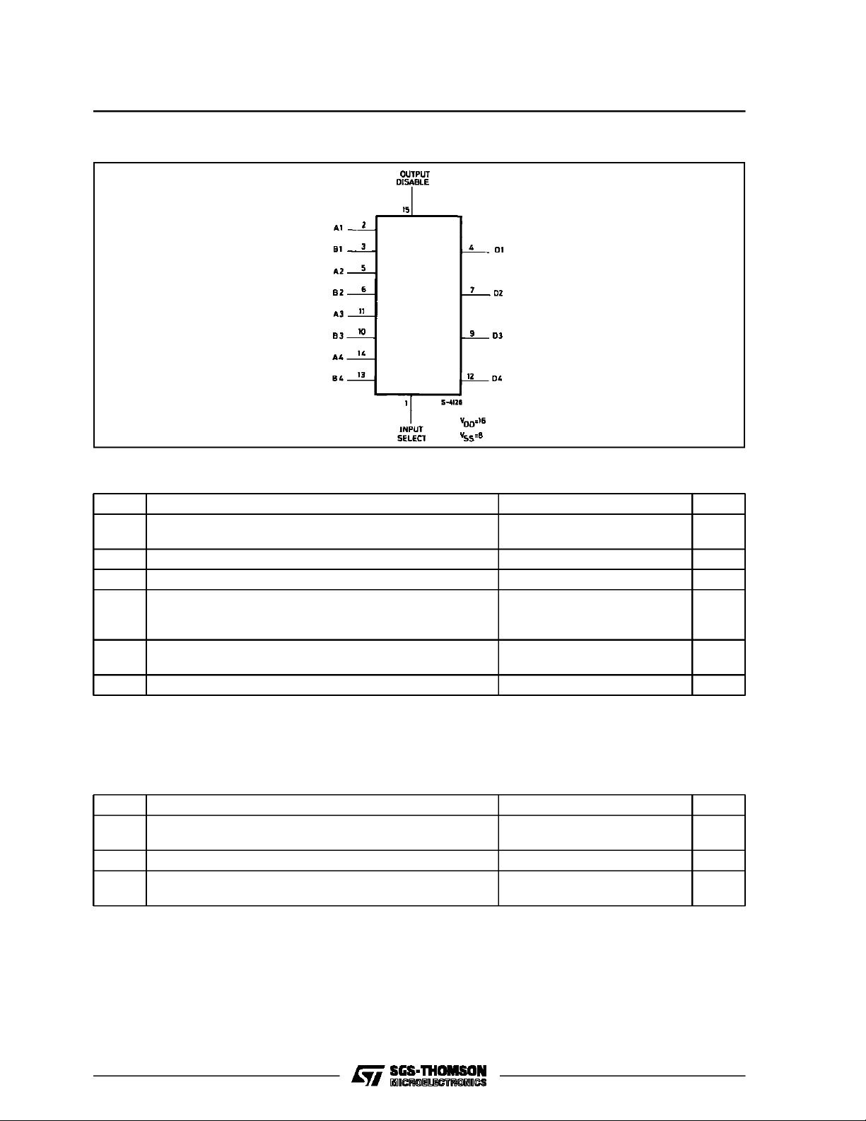
PIN CONNECTIONS
(Plastic Chip Carrier)
C1
June1989
1/11
HCC/HCF40257B
FUN CTIONAL DIAG R A M
ABSOLUTE MAXIMUM RATINGS
Symbol Parameter Value Unit
V
* Supply Voltage :HC C Types
DD
HCF Types
V
Input Voltage – 0.5 to VDD+ 0.5 V
i
I
DC Input Current (any one input) ± 10 mA
I
P
Total Power Dissipation (per package)
tot
Dissipation per Output Transistor
for T
T
Operating Temperature : HCC Types
op
= Full Package-temperature Range
op
HCF Types
T
Stresses above those listed under ”Absolute Maximum Ratings” may cause permanent damage to the device. This is a stress
rating only and functional operation of the device at these or any other conditions above those indicated in the operational sections
of this specification is not implied. Exposure to absolute maximum rating conditions for extended periods may affect device reliability.
* All voltages are with respect to VSS(GND).
Storage Temperature – 65 to + 150 °C
stg
– 0.5 to + 20
– 0.5 to + 18
200
100
– 55 t o + 125
–40to+85
V
V
mW
mW
°C
°C
RECOMMENDED OPERATING CONDITIONS
Symbol Parameter Value Unit
2/11
V
Supply Voltage : HCC Types
DD
HCF Types
V
Input Voltage 0 to V
I
T
Operating Temperature : HCC Types
op
HCF Types
3to18
3to15
DD
– 55 t o + 125
–40to+85
V
V
V
°C
°C
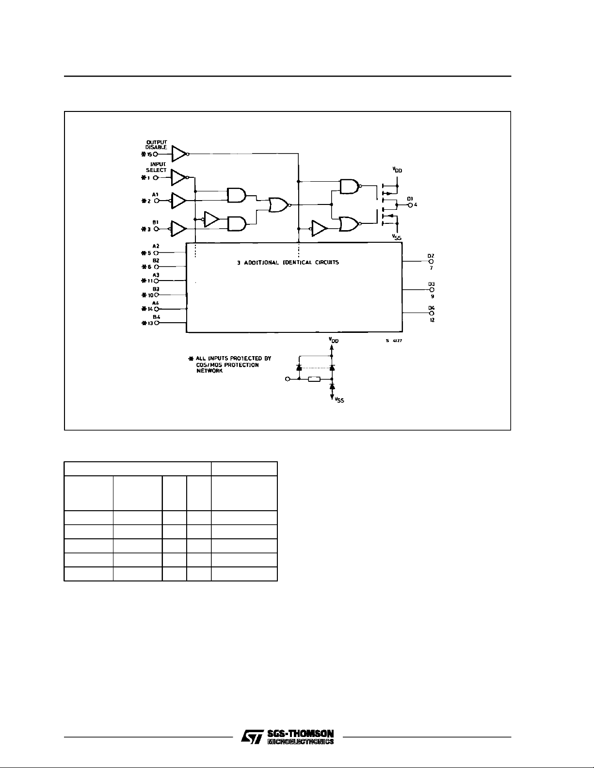
LOGI C DI AGRAM
HCC/HCF40257B
TRUTH TABLE
Inputs Outpu t
3-State
Output
Disable
1XXXZ
000X0
001X1
01X00
01X11
X = Don’t Care
Logic 1 = High
Logic 0 = Low
Z = High impedance.
Select A B D
3/11
HCC/HCF40257B
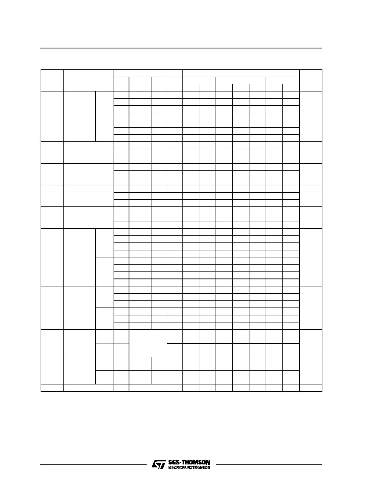
STATIC ELECTRICAL CHARACTERISTICS (over recommended operating conditions)
Test Conditions Value
Symbol Param ete r
(V) (V) (µA) (V)
I
L
Quiescent
Current
HCC
Types
0/ 5 5 1 0.02 1 30
0/10 10 2 0.02 2 60
0/15 15 4 0.02 4 120
0/20 20 20 0.04 20 600
HCF
Types
OH
Output High
V
Voltage
0/ 5 5 4 0.02 4 30
0/10 10 8 0.02 8 60
0/15 15 16 0.02 16 120
0/ 5 < 1 5 4.95 4.95 4.95
0/10 < 1 10 9.95 9.95 9.95
0/15 < 1 15 14.95 14.95 14.95
OL
Output Low
V
Voltage
5/10 < 1 5 0.05 0.05 0.05
10/0 < 1 10 0.05 0.05 0.05
15/0 < 1 15 0.05 0.05 0.05
V
V
I
Input High Voltage 0.5/4.5 < 1 5 3.5 3.5 3.5
IH
Input Low Voltage 4.5/0.5 < 1 5 1.5 1.5 1.5
IL
OH
Output
Drive
Current
HCC
Types
0/ 5 2.5 5 – 2 – 1.6 – 3.2 – 1.15
0/ 5 4.6 5 – 0.64 – 0.51 – 1 – 0.36
0/10 9.5 10 – 1.6 – 1.3 – 2.6 – 0.9
0/15 13.5 15 – 4.2 – 3.4 – 6.8 – 2.4
0/ 5 2.5 5 – 1.53 – 1.36 – 3.2 – 1.1
HCF
Types
0/ 5 4.6 5 – 0.52 – 0.44 – 1 – 0.36
0/10 9.5 10 – 1.3 – 1.1 – 2.6 – 0.9
0/15 13.5 15 – 3.6 – 3.0 – 6.8 – 2.4
OL
Output
Sink
Current
HCC
Types
I
HCF
Types
I
IH,IIL
Input
Leakage
Current
HCC
Types
HCF
Types
IOH,IOL**
*T
*T
The Noise Margin for both ”1” and ”0” level is : 1V min. with VDD= 5V, 2V min. with VDD= 10V, 2.5V min. with VDD= 15V.
** Forced output disable.
3-State
Output
Leakage
Current
C
Input Capacitance Any Input 5 7.5 pF
I
=–55°CforHCC device : – 40°C for HCF device.
Low
= + 125°CforHCC device : + 85°CforHCF device.
High
HCC
Types
HCF
Types
0/ 5 0.4 5 0.64 0.51 1 0.36
0/10 0.5 10 1.6 1.3 2.6 0.9
0/15 1.5 15 4.2 3.4 6.8 2.4
0/ 5 0.4 5 0.52 0.44 1 0.36
0/10 0.5 10 1.3 1.1 2.6 0.9
0/15 1.5 15 3.6 3.0 6.8 2.4
0/18
0/15
0/18 0/18 18 ± 0.4 ±10
0/18 0/18 18 ± 1.0 ±10
V
V
I
O
|IO|V
DD
T
* 25°CT
Low
Min. Max. Min. Typ. Max. Min. Ma x.
1/9 < 1 10 7 7 7
1.5/13.5 < 1 15 11 11 11
9/1 < 1 10 3 3 3
13.5/1.5 < 1 15 4 4 4
18 ± 0.1 ±10
–5
± 0.1 ± 1
Any Input
15 ± 0.3 ±10
–5
± 0.3 ± 1
–4
± 0.4 ± 12
–4
± 1.0 7.5
High
*
Unit
µA
V
V
V
V
mA
mA
µA
µA
4/11
 Loading...