

Datasheet HCF4023BM1, HCF4023BF, HCF4023BEY, HCF4023BC1, HCF4012BM1 Datasheet (SGS Thomson Microelectronics)
...
HCC4011B/12B/23B
HCF4011B/12B/23B
NAND GATES
DESCRIPTION
.PROPAGATIONDELAY TIME = 60ns (typ.) AT
CL= 50pF, VDD= 10V
.BUFFERED INPUTS AND OUTPUTS
.QUIESCENT CURRENT SPECIFIED TO 20V
FOR HCC DEVICE
.INPUT CURRENTOF100nA AT18V AND25°C
FOR HCC DEVICE
.100% TESTEDFOR QUIESCENTCURRENT
.5V, 10V AND 15V PARAMETRIC RATINGS
.MEETSALLREQUIREMENTSOFJEDECTEN-
TATIVE STANDARD No. 13A, ”STANDARD
SPECIFICATIONS FOR DESCRIPTIONOF ”B”
SERIESCMOS DEVICES”
QUAD 2 INPUT HC C/HCF 4011B
DUAL 4 INPUT HCC/HCF 4012B
TRIPLE 3 INPU T HCC / H CF 4023B
June 1989
The HCC4011B, HCC4012B and HCC4023B (ex-
tended temperature range) and HCF4011B,
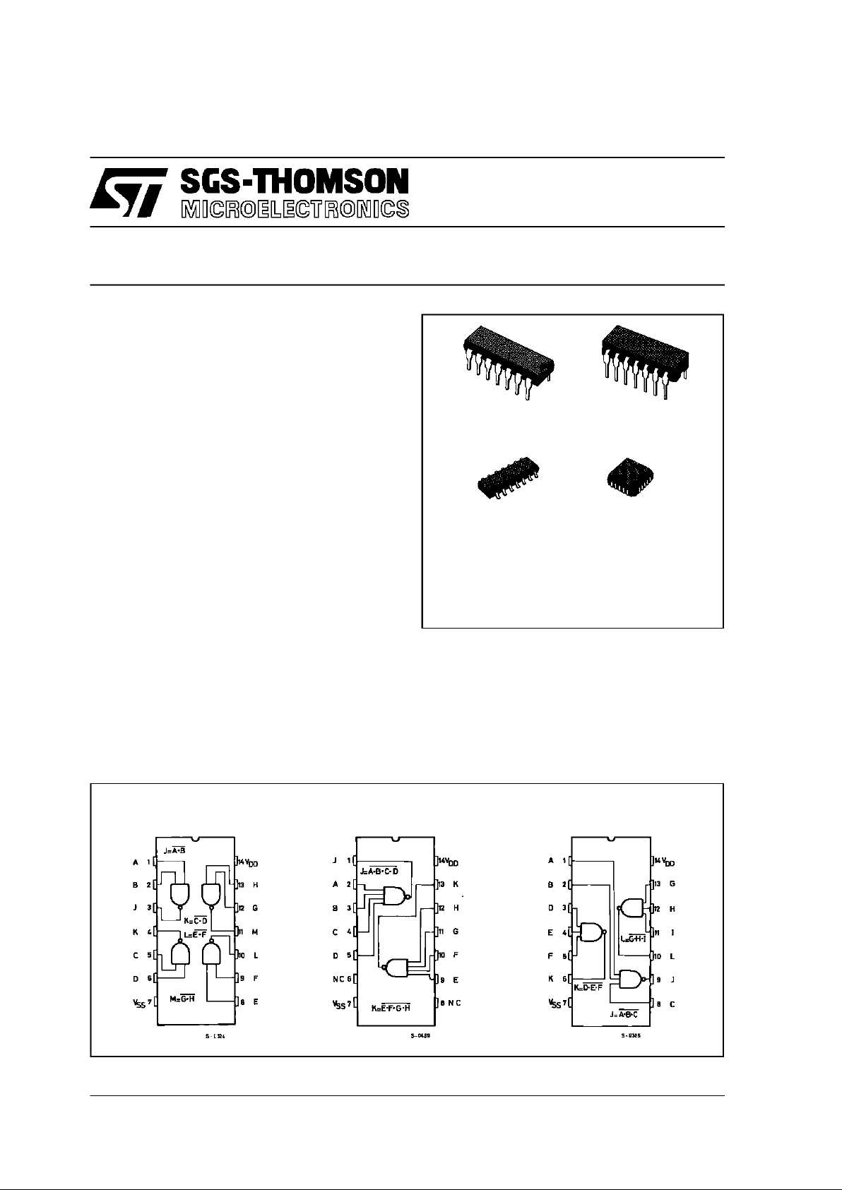
HCF4012B and HCF4023B (intermediate temperature range) are monolithic, integrated circuit, available in 14-lead dual in-line plastic or ceramic
package and plastic micropackage.
The HCC/HCF4011B, HCC/HCF4012B and
HCC/HCF4023B NAND gates provide the system
designer with direct implementation of the NAND
function and supplement the existing family of
COS/MOS gates. All inputs and outputs are buffered.
PIN CONNECTIONS
EY
(Plastic Package)F(Ceramic Frit Seal Package)
M1
(MicroPackage)C1(PlasticChip Carrier)
ORDER CODES :
HCC40XXBF HCF40XXBM1
HCF40XXBEY HCF40XXBC1
4011B 4012B 4023B
1/12
ABSOLUTE M AXI MU M RATI NGS
Symbol Parameter Val ue Unit
V
DD
* Supply Voltage : HCC Types
HCF Types
– 0.5 to + 20
– 0.5 to + 18
V
V
V
i
Input Voltage – 0.5 to VDD+ 0.5 V
I
I
DC Input Current (any one input) ± 10 mA
P
tot
Total Power Dissipation (per package)
Dissipation per Output Transistor
for Top= Full Package-temperature Range
200
100
mW
mW
T
op
Operating Temperature : HCC Types
HCF Types
–55to+125
–40to+85
°C
°C
T
stg
Storage Temperature – 65 to + 150 °C
RECOMMENDED OPERATING CONDITIONS
Symbol Pa ramet er Valu e Un i t
V
DD
Supply Voltage : HC C Types
HCF Types
3to18
3to15
V
V
V
I
Input Voltage 0 to V
DD
V
T
op
Operating Temperature : HCC Types
HCF Types
–55to+125
–40to+85
°C
°C
Stresses above those listed under ”Absolute Maximum Ratings” may cause permanent damage to the device. This is a stress rating only and
functionaloperationofthedeviceattheseoranyotherconditionsabove thoseindicatedintheoperationalsectionsofthisspecificationisnotimplied.
Exposure to absolute maximum rating conditions forexternal periodsmay affectdevice reliability.
* Allvoltage values are referred to VSSpinvoltage.
HCC/H FC4011B/12B/23B
2/12
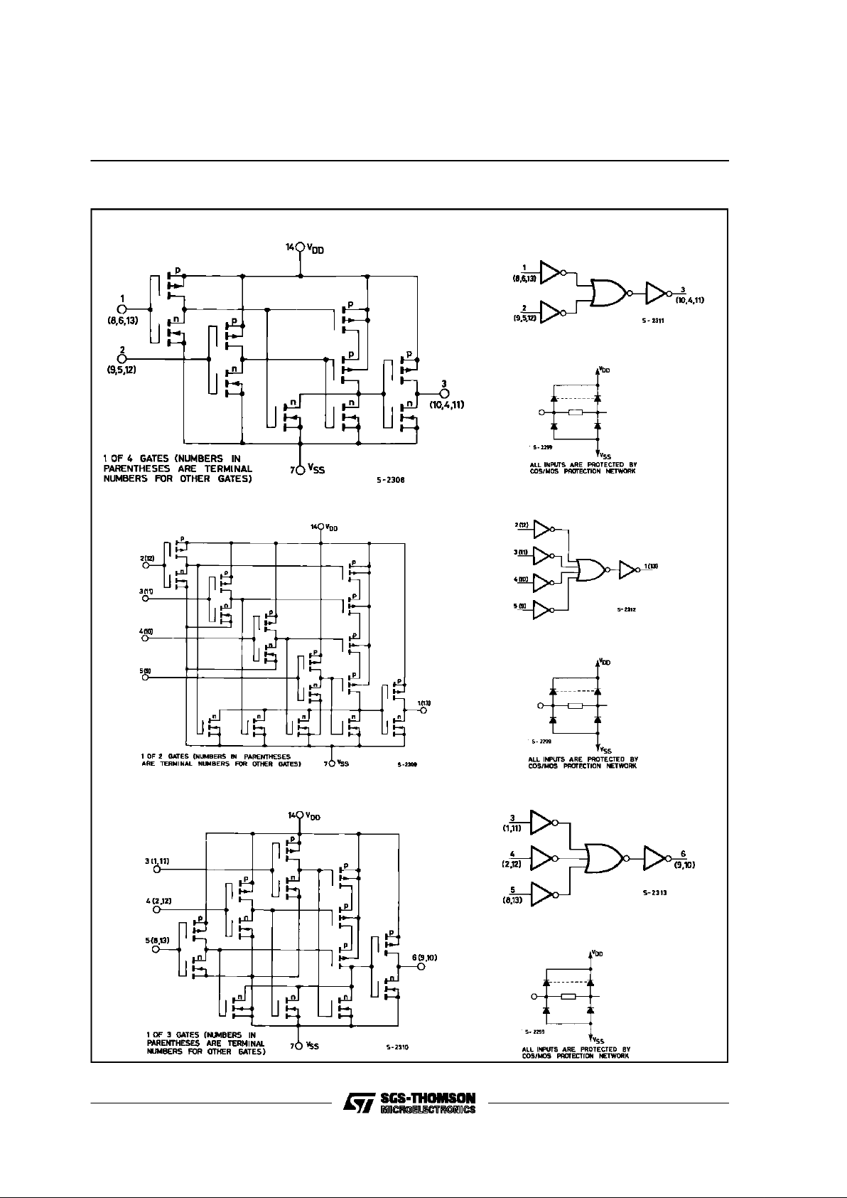
SCHEMATIC AND LOGIC DIAGRAMS
4011B
4023B
4012B
HCC/HCF4011B/12B/23B
3/12
STATIC ELECTRICAL CHARACTERISTICS (over recommended operating conditions)
Test Conditions Valu e
V
I
V
O
|IO|V
DD
T
Low
* 25°CT
High
*
Symbol Parameter
(V) (V) (µA) (V)
Min. Max. Min. Typ. Max. Min. Max.
Unit
I
L
Quiescent
Current
HCC
Types
0/5 5 0.25 0.01 0.25 7.5
µA
0/10 10 0.5 0.01 0.5 15
0/15 15 1 0.01 1 30
0/20 20 5 0.02 5 150
HCF
Types
0/ 5 5 1 0.01 1 7.5
0/10 10 2 0.01 2 15
0/15 15 4 0.01 4 30
V
OH
Output High
Voltage
0/5 < 1 5 4.95 4.95 4.95
V
0/10 < 1 10 9.95 9.95 9.95
0/15 < 1 15 14.95 14.95 14.95
V
OL
Output Low
Voltage
5/0 < 1 5 0.05 0.05 0.05
V
10/0 < 1 10 0.05 0.05 0.05
15/0 < 1 15 0.05 0.05 0.05
V
IH
Input High
Voltage
0.5/4.5 < 1 5 3.5 3.5 3.5
V
1/9 < 1 10 7 7 7
1.5/13.5 < 1 15 11 11 11
V
IL
Input Low
Voltage
4.5/0.5 < 1 5 1.5 1.5 1.5
V
9/1 < 1 10 3 3 3
13.5/1.5 < 1 15 4 4 4
I
OH
Output
Drive
Current
HCC
Types
0/5 2.5 5 – 2 – 1.6 – 3.2 – 1.15
mA
0/5 4.6 5 – 0.64 – 0.51 – 1 – 0.36
0/10 9.5 10 – 1.6 – 1.3 – 2.6 – 0.9
0/15 13.5 15 – 4.2 – 3.4 – 6.8 – 2.4
HCF
Types
0/5 2.5 5 – 1.53 – 1.36 – 3.2 – 1.1
0/5 4.6 5 – 0.52 – 0.44 – 1 – 0.36
0/10 9.5 10 – 1.3 – 1.1 – 2.6 – 0.9
0/15 13.5 15 – 3.6 – 3.0 – 6.8 – 2.4
I
OL
Output
Sink
Current
HCC
Types
0/5 0.4 5 0.64 0.51 1 0.36
mA
0/10 0.5 10 1.6 1.3 2.6 0.9
0/15 1.5 15 4.2 3.4 6.8 2.4
HCF
Types
0/5 0.4 5 0.52 0.44 1 0.36
0/10 0.5 10 1.3 1.1 2.6 0.9
0/15 1.5 15 3.6 3.0 6.8 2.4
I
IH,IIL
Input
Leakage
Current
HCC
Types
0/18
Any Input
18 ± 0.1 ±10–5± 0.1 ± 1
µA
HCF
Types
0/15 15 ± 0.3 ±10
–5
± 0.3 ± 1
C
I
Input Capacitance Any Input 5 7.5 pF
*T
LOW
=–55°Cfor HCC device : – 40°CforHCF device.
*T
HIGH
=+ 125°C forHCC device : + 85°C for HCF device.
TheNoise Margin for both”1” and ”0” level is : 1V min.with VDD=5V, 2V min.with VDD= 10V,2.5V withVDD= 15V.
HCC/H FC4011B/12B/23B
4/12

TEST CIRCUITS
QuiescentDevice Current. Noise Immunity.
Input Leakage Current.
DYNAMIC ELECTRICAL CHARACTERISTICS(T
amb
=25°C, CL= 50pF, RL= 200kΩ,
typical temperature coefficient for all VDDvalues is 0.3%/°C, all input rise and fall times = 20ns)
Val ue
Symbol Parameter
Test Conditions
V
DD
(V) Min. Typ. Max.
Unit
t
PLH,tPHL
Propagation Delay Time 5 125 250
ns
10 60 120
15 45 90
t
THL,tTLH
Transition Time 5 100 200
ns
10 50 100
15 40 80
HCC/HCF4011B/12B/23B
5/12

Minimum Output High (source) Current Characteristics.
Minimum Output Low(sink) Current Characteristics.
TypicalOutputHigh (source) Current Characteristics.
TypicalOutput Low (sink) Current Characteristics.
TypicalPropagation Delay Time per Gate as a
Function of Load Capacitance.
TypicalTransition Time vs. Load Capacitance.
HCC/H FC4011B/12B/23B
6/12

TypicalVoltage Transfer Characteristics. Typical Power Dissipation/gate vs Frequency.
HCC/HCF4011B/12B/23B
7/12

Plastic DIP14 MECHANICAL DATA
DIM.
mm inch
MIN. TYP. MAX. MIN. TYP. MAX.
a1 0.51 0.020
B 1.39 1.65 0.055 0.065
b 0.5 0.020
b1 0.25 0.010
D 20 0.787
E 8.5 0.335
e 2.54 0.100
e3 15.24 0.600
F 7.1 0.280
I 5.1 0.201
L 3.3 0.130
Z 1.27 2.54 0.050 0.100
P001A
HCC/H FC4011B/12B/23B
8/12

Ceramic DIP14/1 MECHANICAL DATA
DIM.
mm inch
MIN. TYP. MAX. MIN. TYP. MAX.
A 20 0.787
B 7.0 0.276
D 3.3 0.130
E 0.38 0.015
e3 15.24 0.600
F 2.29 2.79 0.090 0.110
G 0.4 0.55 0.016 0.022
H 1.17 1.52 0.046 0.060
L 0.22 0.31 0.009 0.012
M 1.52 2.54 0.060 0.100
N 10.3 0.406
P 7.8 8.05 0.307 0.317
Q 5.08 0.200
P053C
HCC/HCF4011B/12B/23B
9/12

SO14 MECHANICAL DATA
DIM.
mm inch
MIN. TYP. MAX. MIN. TYP. MAX.
A 1.75 0.068
a1 0.1 0.2 0.003 0.007
a2 1.65 0.064
b 0.35 0.46 0.013 0.018
b1 0.19 0.25 0.007 0.010
C 0.5 0.019
c1 45° (typ.)
D 8.55 8.75 0.336 0.344
E 5.8 6.2 0.228 0.244
e 1.27 0.050
e3 7.62 0.300
F 3.8 4.0 0.149 0.157
G 4.6 5.3 0.181 0.208
L 0.5 1.27 0.019 0.050
M 0.68 0.026
S8°(max.)
P013G
HCC/H FC4011B/12B/23B
10/12

PLCC20 MECHANICAL DATA
DIM.
mm inch
MIN. TYP. MAX. MIN. TYP. MAX.
A 9.78 10.03 0.385 0.395
B 8.89 9.04 0.350 0.356
D 4.2 4.57 0.165 0.180
d1 2.54 0.100
d2 0.56 0.022
E 7.37 8.38 0.290 0.330
e 1.27 0.050
e3 5.08 0.200
F 0.38 0.015
G 0.101 0.004
M 1.27 0.050
M1 1.14 0.045
P027A
HCC/HCF4011B/12B/23B
11/12

Information furnished is believed to be accurate and reliable. However, SGS-THOMSON Microelectronics assumes no responsability for the
consequences of use of such information nor for any infringement of patents or other rights of third parties which may results from its use. No
license isgranted byimplication or otherwiseunder any patentor patent rights of SGS-THOMSON Microelectronics. Specificationsmentioned
in this publication are subject to changewithout notice. This publication supersedes and replaces all information previously supplied.
SGS-THOMSON Microelectronicsproductsare notauthorized for use ascritical componentsinlife supportdevices orsystemswithout express
written approval of SGS-THOMSON Microelectonics.
1994 SGS-THOMSON Microelectronics - All RightsReserved
SGS-THOMSON Microelectronics GROUP OF COMPANIES
Australia - Brazil - France - Germany - Hong Kong - Italy - Japan - Korea - Malaysia - Malta - Morocco - The Netherlands -
Singapore - Spain - Sweden - Switzerland - Taiwan - Thailand - UnitedKingdom - U.S.A
HCC/H FC4011B/12B/23B
12/12
 Loading...