


. FOUR 4-BIT REGISTERS
.ONE INPUT AND TWO OUTPUT BUSES
.UNLIMITED EXPANSION IN BIT AND WORD
DIRECTIONS
.DATA LINESHAVE LATCHED INPUTS
.3-STATE OUTPUTS
.SEPARATE CONTROL OF EACH BUS,
ALLOWING SIMULTANEOUS INDEPENDENT
READINGOF ANY OF FOUR REGISTERSON
BUSAANDBUSBANDINDEPENDENTWRITING INTOANY OF THE FOUR REGISTERS
.40108B IS PIN-COMPATIBLE WITH INDUS-
TRY TYPEMC14580
.STANDARDIZED, SYMMETRICAL OUTPUT
CHARACTERISTICS
.QUIESCENT CURRENT SPECIFIED AT 20V
FOR HCC DEVICE
.5V, 10V,AND 15V PARAMETRIC RATINGS
.INPUT CURRENTOF100nAAT 18V AND25°C
FOR HCC DEVICE
.100% TESTEDFOR QUIESCENTCURRENT
.MEETSALLREQUIREMENTSOFJEDECTEN-
TATIVESTANDARDN°13A,”STANDARDSPECIFICATIONS FOR DESCRIPTION OF ”B”
SERIESCMOS DEVICES”
HCC/H CF4 02 08B
4 x 4 MULTIPORT REGISTER
BEY
(Plastic Package)BF(Ceramic Frit SealPackage)
BM1
(MicroPackage)
ORDER CODES :
HCC40208BF HCF40208BEY
HCF40208BM1
PIN CONNECTIONS
DESCRIPT ION
TheHCC40208B (extended temperature range) and
HCF40208B (intermediate temperature range) are
monolithic integrated circuits, available in 24-lead dual
in-line plastic or ceramic package and plastic micro
package. The HCC/HCF40208B is a 4 x 4 multiport
register containing four 4-bit registers, write address
decoder, two separate read address decoders, and
two3-state output buses. When the ENABLEinput is
low,the corresponding output bus is switched, independently of theclock to ahigh-impedance state. The
high-impedance third state provides the outputs with
the capability of being connected to the bus lines in a
bus-organized systemwithout the need forinterface or
pull-up components. When the WRITE ENABLE input
is high, all data input linesare latched onthe positive
transitionof theCLOCKand thedata isentered into the
wordselectedbythewriteaddresslines. When WRITE
ENABLE is low, the CLOCKis inhibited and no new
dataisentered. Ineither case, the contents ofany word
may be accessed via the read address lines independent ofthestate of the CLOCKinput.
June1989
1/13

HCC/HCF40208B
FUN CTIONAL DIAG R A M
ABSOLUTE M AXI MUM RATI N GS
Symbol Parameter Value Unit
V
* Supply Voltage :HCC Types
DD
HCF Types
V
Input Voltage – 0.5 to VDD+ 0.5 V
i
I
DC Input Current (any one input) ± 10 mA
I
P
Total Power Dissipation (per package)
tot
Dissipation per Output Transistor
for T
T
Operating Temperature : HCC Types
op
= Full Package-temperature Range
op
HCF Types
T
Stresses above those listed under ”Absolute Maximum Ratings” may cause permanent damage to the device. This is a stress
rating only and functional operation of the device at these or any other conditions above those indicated in the operational sections
of this specification is not implied. Exposure to absolute maximum rating conditions for external periods may affect device reliability.
* All voltages are with respect to VSS(GND).
Storage Temperature – 65 to + 150 °C
stg
– 0.5 to + 20
– 0.5 to + 18
200
100
– 55 t o + 125
–40to+85
V
V
mW
mW
°C
°C
RECOMMENDED OPERATING CO NDITIONS
Symbol Parameter Value Unit
V
T
2/13
Supply Voltage : HCC Types
DD
HCF Types
V
Input Voltage 0 to V
I
Operating Temperature : HCC Types
op
HCF Types
3to18
3to15
DD
– 55 t o + 125
–40to+85
V
V
V
°C
°C

SCHEM ATIC DIAGRAM
HCC/HCF40208B
3/13

HCC/HCF40208B
LOGI C DI AG RAM
TIM ING D IAG R AM
4/13

TRUTH TABLE
HCC/HCF40208B
Clock
–
/
–
–
/
–
Write
Enable
Write1Write0Read1ARead0ARead1BRead0BEnab l eAEnab l e
B
D
n
Q
nA
1S1S2S1S2S1S211111
1S1S2S1S2S1S211000
X X XXXXXX 0 0 X Z Z
–
/
–
–
/
–
1 000110 1 1
0 000110 1 1
X X XX1001 1 1 X
–
\
–
1 = HIGH LEVEL, 0 = LOW LEVEL, X = DON’T CARE, Z = HIGH IMPEDANCE.
S1 and S2 refer to input strates of either 1 or 0.
X XXXXXX 1 1 X NC NC
D
to
n
Word 0
Word 0
Not
Altered
Word 1
Out
Word 1
Out
Word 2
Out
Word 2
Word 2
Word 1
STATIC ELECTRICAL CHARACTERISTICS (over recommended operating conditions)
Test Conditions Valu e
Symbol Parameter
(V) (V) (µA) (V)
I
L
Quiescent
Current
HCC
Types
0/ 5 5 5 0.04 5 150
0/10 10 10 0.04 10 300
0/15 15 20 0.04 20 600
0/20 20 100 0.08 100 3000
HCF
Types
OH
Output High
V
Voltage
0/ 5 5 20 0.04 20 150
0/10 10 40 0.04 40 300
0/15 15 80 0.04 80 600
0/ 5 < 1 5 4.95 4.95 4.95
0/10 < 1 10 9.95 9.95 9.95
0/15 < 1 15 14.95 14.95 14.95
OL
Output Low
V
Voltage
5/0 < 1 5 0.05 0.05 0.05
10/0 < 1 10 0.05 0.05 0.05
15/0 < 1 15 0.05 0.05 0.05
V
IH
Input High
Voltage
IL
Input Low
V
Voltage
I
OH
Output
Drive
Current
HCC
Types
0/ 5 2.5 5 – 2 – 1.6 – 3.2 – 1.15
0/ 5 4.6 5 – 0.64 – 0.51 – 1 – 0.36
0/10 9.5 10 – 1.6 – 1.3 – 2.6 – 0.9
0/15 13.5 15 – 4.2 – 3.4 – 6.8 – 2.4
0/ 5 2.5 5 – 1.53 – 1.36 – 3.2 – 1.1
HCF
Types
0/ 5 4.6 5 – 0.52 – 0.44 – 1 – 0.36
0/10 9.5 10 – 1.3 – 1.1 – 2.6 – 0.9
0/15 13.5 15 – 3.6 – 3.0 – 6.8 – 2.4
*T
=–55°CforHCC device : – 40°C for HCF device.
Low
*T
= + 125°CforHCC device : + 85°CforHCF device.
High
The Noise Margin for both ”1” and ”0” level is : 1V min. with VDD= 5V, 2V min. with VDD= 10V, 2.5V min. with VDD= 15V.
** Forced output disable.
V
V
I
O
|IO|V
DD
T
* 25°CT
Low
Min. Max. Min. Typ. M ax. Min. Max.
0.5/4.5 < 1 5 3.5 3.5 3.5
1/9 < 1 10 7 7 7
1.5/13.5 < 1 15 11 11 11
4.5/0.5 < 1 5 1.5 1.5 1.5
9/1 < 1 10 3 3 3
13.5/1.5 < 1 15 4 4 4
High
*
Q
Out
Out
Out
Unit
µA
mA
nB
V
V
V
V
5/13

HCC/HCF40208B
STATIC ELECTRICAL CHARACTERISTICS (continued)
Test Conditions Valu e
Symbol Parameter
(V) (V) (µA) (V)
OL
Output
Sink
Current
HCC
Types
I
HCF
Types
I
IH,IIL
Input
Leakage
Current
HCC
Types
HCF
Types
IOH,IOL**
*T
*T
The Noise Margin for both ”1” and ”0” level is : 1V min. with VDD= 5V, 2V min. with VDD= 10V, 2.5V min. with VDD= 15V.
** Forced output disable.
3-State
Output
Leakage
Current
C
Input Capacitance Any Input 5 7.5 pF
I
=–55°CforHCC device : – 40°C for HCF device.
Low
= + 125°CforHCC device : + 85°CforHCF device.
High
HCC
Types
HCF
Types
0/ 5 0.4 5 0.64 0.51 1 0.36
0/10 0.5 10 1.6 1.3 2.6 0.9
0/15 1.5 15 4.2 3.4 6.8 2.4
0/ 5 0.4 5 0.52 0.44 1 0.36
0/10 0.5 10 1.3 1.1 2.6 0.9
0/15 1.5 15 3.6 3.0 6.8 2.4
0/18
0/15
0/18 0/18
0/15 0/15
V
I
V
O
Any Input
|IO|V
DD
T
Low
Min. Max. Min. Typ. M ax. Min. Max.
18
± 0.1 ±10
15 ± 0.3 ±10
18 ± 0.4 ±10
15 ± 1.0 ±10
* 25°CT
–5
± 0.1 ± 1
–5
± 0.3 ± 1
–4
± 0.4 ± 12
–4
± 1.0 ± 7.5
High
*
Unit
mA
µA
µA
DYNAMIC ELECTRICAL CHARACTERISTICS (T
=25°C, CL= 50pF, RL= 200kΩ,
amb
typical temperature coefficient for all VDDvalues is 0.3%/°C, all input rise and fall time = 20ns)
Symbol Parameter
t
,
PHL
t
PLH
Propagation Delay Time :
Clock to Write Enable to Q
Read or Write Address to Q 5 300 600
,
t
PZH
t
t
PZL
t
t
THL
t
TLH
t
setup
PHZ
PL Z
3-state Disable Delay Time 5 100 200
,
3-State Disable Delay time 5 130 260
,
Output Transition Time 5 100 200
Setup Time
Data to Clock t
s(D)
Write Enable to Clock t
Write Address to Clock t
s(WE)
s(WA)
Test Conditions Value
(V) Min. Typ. Ma x.
V
DD
5360720
10 140 280
15 100 200
10 120 240
15 85 170
10 50 100
15 40 80
10 60 120
15 50 100
10 50 100
15 40 80
50–95
10 0 – 35
15 0 – 20
5 250 125
10 100 50
15 70 35
5 250 125
10 100 50
15 70 35
Unit
ns
ns
ns
ns
ns
ns
ns
ns
6/13

DYNAMIC ELECTRICAL CHARACTERISTICS (continued)
Symbol Parameter
t
t
hold
r,tf
Clock Rise and Fall Time 5 15
Hold Time
Data to Clock t
h(D)
Write Enable to Clock t
Write Address to Clock t
t
Clock Pulse Width
W
Clock or Write Enable t
Write Address t
f
CL
Maximum Clock Input Frequency 5 1.5 3
W(WA )
h(WE)
s(WA)
W(CL)
Test Conditions Value
HCC/HCF40208B
(V) Min. Typ. Ma x.
V
DD
10 5
15 5
5 220 110
10 100 50
15 80 40
5 270 135
10 130 65
15 80 40
5 330 165
10 140 70
15 90 45
5 350 175
10 130 65
15 90 45
5 300 150
10 150 75
15 90 45
10 3.5 7
15 4.5 9
Unit
µs
ns
ns
ns
ns
MHz
OutputLow (sink) Current Characteristics. OutputHigh (source) Current Characteristics.
7/13

HCC/HCF40208B
TypicalPropagation Delay Time vs.Load Capacitance(CL or WE to Q).
TypicalDynamicPower Dissipation vs. Input Frequency.
TypicalTransition Time vs. Load Capacitance.
TEST CIRCUITS
Output-enable-delay-times and Waveforms.
8/13

Power-dissipation and Waveforms.
QuiescentDevice Current. InputVoltage.
HCC/HCF40208B
Input Current.
9/13

HCC/HCF40208B
Plastic DIP24 (0.25) MECHANICAL DATA
DIM.
MIN. TYP. MAX. MIN. TYP. MAX.
a1 0.63 0.025
b 0.45 0.018
b1 0.23 0.31 0.009 0.012
b2 1.27 0.050
D 32.2 1.268
E 15.2 16.68 0.598 0.657
e 2.54 0.100
e3 27.94 1.100
F 14.1 0.555
I 4.445 0.175
L 3.3 0.130
mm inch
10/13
P043A
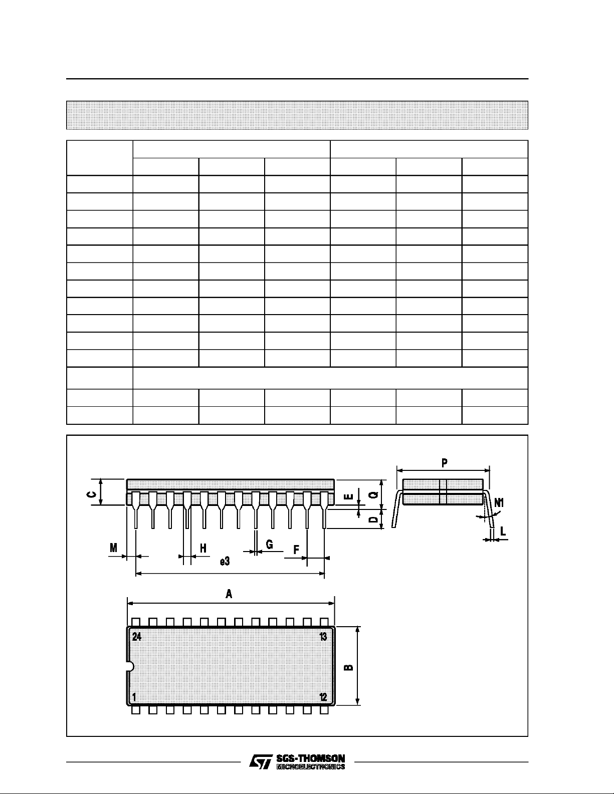
Ceramic DIP24 MECHANICAL DATA
HCC/HCF40208B
DIM.
MIN. TYP. MAX. MIN. TYP. MAX.
A 32.3 1.272
B 13.05 13.36 0.514 0.526
C 3.9 5.08 0.154 0.200
D 3 0.118
E 0.5 1.78 0.020 0.070
e3 27.94 1.100
F 2.29 2.79 0.090 0.110
G 0.4 0.55 0.016 0.022
I 1.17 1.52 0.046 0.060
L 0.22 0.31 0.009 0.012
M 1.52 2.49 0.060 0.098
N1
P 15.4 15.8 0.606 0.622
Q 5.71 0.225
4° (min.), 15° (max.)
mm inch
P058C
11/13

HCC/HCF40208B
SO24 MECHANICAL DATA
DIM.
MIN. TYP. MAX. MIN. TYP. MAX.
A 2.65 0.104
a1 0.10 0.20 0.004 0.007
a2 2.45 0.096
b 0.35 0.49 0.013 0.019
b1 0.23 0.32 0.009 0.012
C 0.50 0.020
c1 45° (typ.)
D 15.20 15.60 0.598 0.614
E 10.00 10.65 0.393 0.420
e 1.27 0.05
e3 13.97 0.55
F 7.40 7.60 0.291 0.299
L 0.50 1.27 0.19 0.050
S8°(max.)
mm inch
L
A
a2
b
e3
D
24 13
112
e
F
s
a1
c1
b1
C
E
12/13

HCC/HCF40208B
Information furnished isbelieved tobe accurate and reliable.However, SGS-THOMSON Microelectronics assumes no responsability for the
consequences of use of suchinformation nor for anyinfringement of patents orother rightsof third parties which may results fromits use. No
license is grantedby implication or otherwise underany patentor patent rights ofSGS-THOMSON Microelectronics. Specificationsmentioned
in this publicationare subject to changewithout notice.Thispublication supersedes and replaces all informationpreviously supplied.
SGS-THOMSON Microelectronicsproductsare notauthorized foruse ascritical componentsin life supportdevices or systemswithout express
written approval of SGS-THOMSON Microelectonics.
1994SGS-THOMSON Microelectronics- All RightsReserved
Australia - Brazil - France - Germany - Hong Kong - Italy- Japan - Korea - Malaysia -Malta - Morocco - The Netherlands-
Singapore - Spain - Sweden- Switzerland - Taiwan - Thailand - UnitedKingdom - U.S.A
SGS-THOMSON Microelectronics GROUP OF COMPANIES
13/13
 Loading...