

SGS Thomson Microelectronics HCF4019B Datasheet
HCC/HCF4019B
QUAD AND/OR SELECT GATE
.MEDIUM SPEED OPERATION : t
60ns (typ.) AT CL=50pF, VDD=10V
PHL=tPLH
.STANDARDIZED, SYMMETRICAL OUTPUT
CHARACTERISTICS
.QUIESCENT CURRENT SPECIFIED TO 20V
FOR HCC DEVICE
.5V, 10V,AND 15V PARAMETRIC RATINGS
.INPUTCURRENTOF100nA AT18V AND25°C
FOR HCC DEVICE
.100% TESTEDFOR QUIESCENTCURRENT
.MEETSALLREQUIREMENTSOFJEDECTEN-
TATIVE STANDARD No. 13A, ”STANDARD
SPECIFICATIONS FOR DESCRIPTIONOF ”B”
SERIESCMOS DEVICES”
=
EY
(Plastic Package)
M1
(MicroPackage )
ORDERCODES :
HCC4019BF HCF4019BM1
HCF4019BEY HCF4019BC1
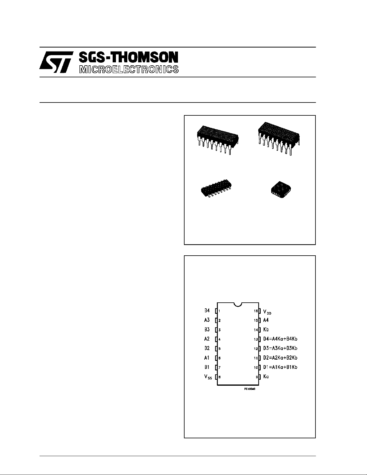
PIN CON NEC TI O NS
(CeramicFrit Seal Package)
(Plastic Chip Carrier)
F
C1
DESCRIPTION
TheHCC4019B(extended temperature range) and
HCF4019B (intermediate temperature range) are
monolithic integrated circuit, available in 16-lead
dual in-line plastic or ceramic package and plastic
micro package.
The HCC/HCF4019B types are comprised of four
AND/ORselectgate configurations, eachconsisting
oftwo2-inputANDgatesdriving asingle2-input OR
gate. Selection is accomplished by control bits K
and Kb. In additionto selection of either channel A
or channelBinformation, the controlbits can be applied simultaneously to accomplish the logicalA+B
function.
June 1989
a
1/13
HCC/HCF4019B
ABSOLUTE M AXIMU M RATINGS
Symbol Parame ter Val ue Unit
V
* Supply Voltage :HCC Types
DD
HCF Types
V
Input Voltage – 0.5 to VDD+ 0.5 V
i
I
DC Input Current (any one input) ± 10 mA
I
P
Total Power Dissipation (per package)
tot
Dissipation per Output Transistor
for Top= Full Package-temperature Range
T
Operating Temperature : HCC Types
op
HCF Types
T
Stresses above those listed under ”Absolute Maximum Ratings” may cause permanent damage to the device. This is a stress
rating only and functional operation of the device at these or any other conditions above those indicated in the operational sections of this specification is not implied. Exposure to absolute maximum rating conditions for external periods may affect device
reliability.
* All voltage values are referred to VSSpin voltage.
Storage Temperature – 65 to + 150 °C
stg
RECOMMENDED OPERATING CONDITIONS
Symbol Parameter Value Unit
V
T
Supply Voltage : HCC Types
DD
HCF Types
V
Input Voltage 0 to V
I
Operating Temperature : HCC Types
op
HCF Types
– 0.5to + 20
– 0.5to + 18
200
100
–55to+125
–40to+85
3to18
3to15
DD
– 55 to + 125
–40to+85
V
V
mW
mW
°C
°C
V
V
V
°C
°C
2/13
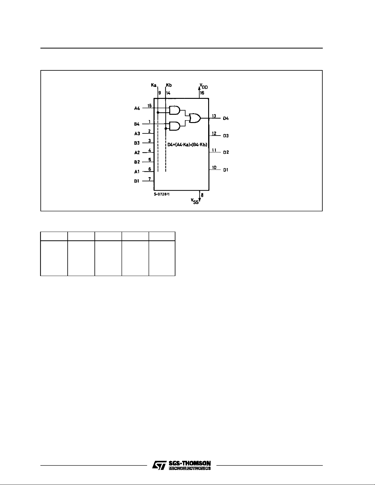
LOGIC DIAGRAMS
4019B
HCC/HCF4019B
TRUTH TABLE
Ka Kb An Bn DN
1
1
X
X
0
X = Don’t care.
X
X
1
1
0
1
0
X
X
X
X
X
1
0
X
1
0
1
0
0
3/13
HCC/HCF4019B
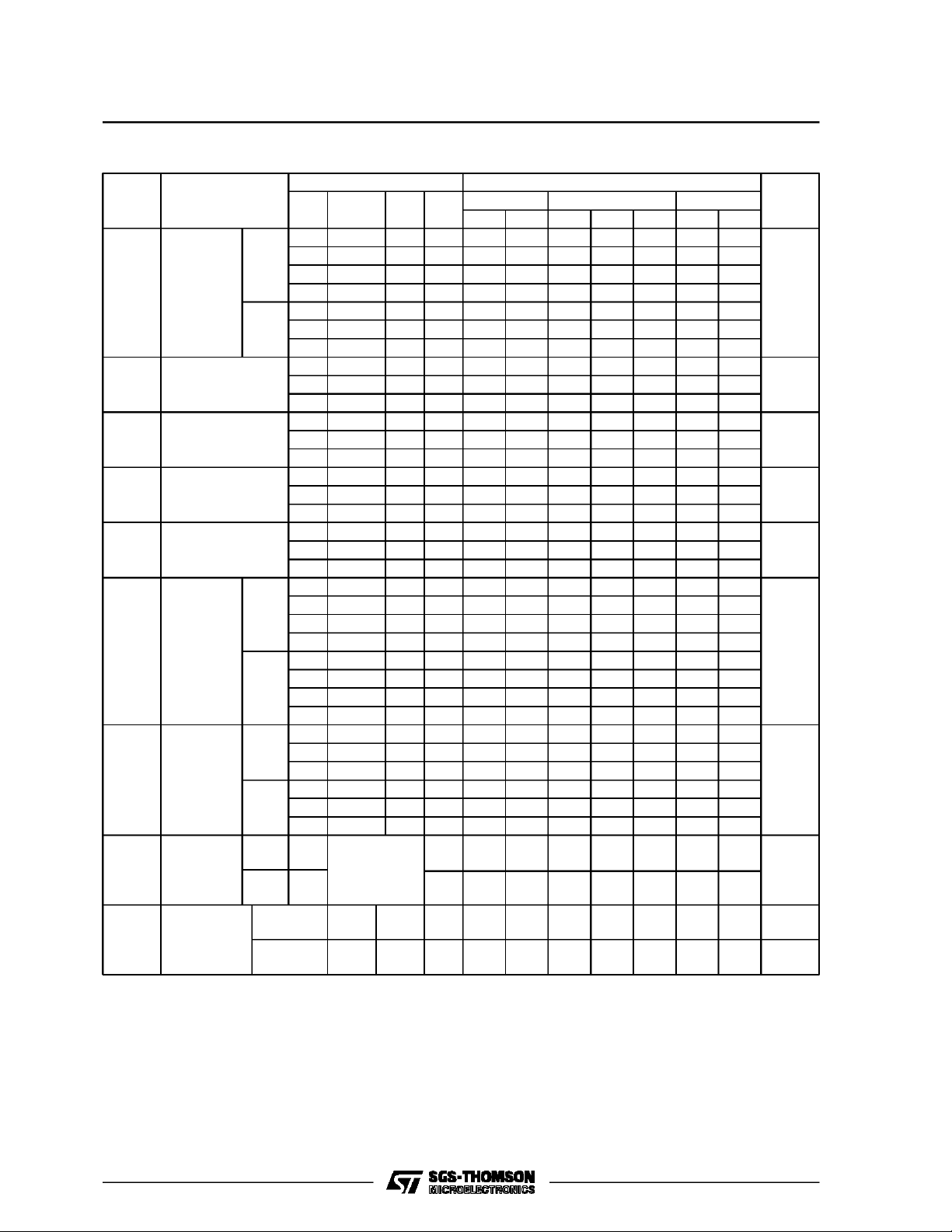
STATIC ELECTRICAL CHARACTERISTICS(over recommended operating conditions)
Test Conditions Valu e
Symbol Parameter
(V) (V) (µA) (V)
I
L
Quiescent
Current
HCC
Types
0/ 5 5 1 0.02 1 30
0/10 10 2 0.02 2 60
0/15 15 4 0.02 4 120
0/20 20 20 0.04 20 600
HCF
Types
OH
Output High
V
Voltage
0/ 5 5 4 0.02 4 30
0/10 10 8 0.02 8 60
0/15 15 16 0.02 16 120
0/ 5 < 1 5 4.95 4.95 4.95
0/10 < 1 10 9.95 9.95 9.95
0/15 < 1 15 14.95 14.95 14.95
V
OL
Output Low
Voltage
5/0 < 1 5 0.05 0.05 0.05
10/0 < 1 10 0.05 0.05 0.05
15/0 < 1 15 0.05 0.05 0.05
IH
Input High
V
Voltage
IL
Input Low
V
Voltage
OH
Output
Drive
Current
HCC
Types
I
0/ 5 2.5 5 – 2 – 1.6 – 3.2 – 1.15
0/ 5 4.6 5 – 0.64 – 0.51 – 1 – 0.36
0/10 9.5 10 – 1.6 – 1.3 – 2.6 – 0.9
0/15 13.5 15 – 4.2 – 3.4 – 6.8 – 2.4
0/ 5 2.5 5 – 1.53 – 1.36 – 3.2 – 1.1
HCF
Types
0/ 5 4.6 5 – 0.52 – 0.44 – 1 – 0.36
0/10 9.5 10 – 1.3 – 1.1 – 2.6 – 0.9
0/15 13.5 15 – 3.6 – 3.0 – 6.8 – 2.4
I
OL
I
IH,IIL
Output
Sink
Current
Input
Leakage
Current
HCC
Types
HCF
Types
HCC
Types
HCF
0/ 5 0.4 5 0.64 0.51 1 0.36
0/10 0.5 10 1.6 1.3 2.6 0.9
0/15 1.5 15 4.2 3.4 6.8 2.4
0/ 5 0.4 5 0.52 0.44 1 0.36
0/10 0.5 10 1.3 1.1 2.6 0.9
0/15 1.5 15 3.6 3.0 6.8 2.4
0/18
0/15
Types
C
I
Input
Capacitance
All A and B
Inputs
Ka and Kb
Inputs
*T
=–55°CforHCC device : – 40°CforHCF device.
Low
*T
= + 125°CforHCC device : + 85°CforHCF device.
High
TheNoiseMarginfor both ”1” and ”0” level is : 1V min.with VDD= 5V, 2Vmin. withVDD= 10V, 2.5 V min.with VDD=15V.
V
V
I
O
|IO|V
DD
T
* 25°CT
Low
Min. Max. Min. Typ. Max. Min. Max.
0.5/4.5 < 1 5 3.5 3.5 3.5
1/9 < 1 10 7 7 7
1.5/13.5 < 1 15 11 11 11
4.5/0.5 < 1 5 1.5 1.5 1.5
9/1 < 1 10 3 3 3
13.5/1.5 < 1 15 4 4 4
–5
± 0.1 ± 1
±10
–5
± 0.3 ± 1
±10
Any Input
18 ± 0.1
15 ± 0.3
5 7.5 pF
10 15 p F
High
Unit
*
µA
V
V
V
V
mA
mA
µA
4/13
 Loading...