

PRESETTABLE DIVIDE-BY-N COUNTER
.MEDIUM SPEED OPERATION - 10MHz (typ.)
AT VDD–VSS= 10V
.FULLYSTATIC OPERATION
.QUIESCENT CURRENT SPECIFIED TO 20V
FOR HCC DEVICE
.STANDARDIZED SYMMETRICAL OUTPUT
CHARACTERISTICS
.INPUT CURRENTOF100nA AT18VAND25°C
FOR HCC DEVICE
.100% TESTEDFOR QUIESCENTCURRENT
.5V, 10V,AND 15VPARAMETRIC RATINGS
.MEETSALLREQUIREMENTSOFJEDECTEN-
TATIVE STANDARD No13A, ”STANDARD
SPECIFICATIONS FOR DESCRIPTIONOF ”B”
SERIESCMOS DEVICES”
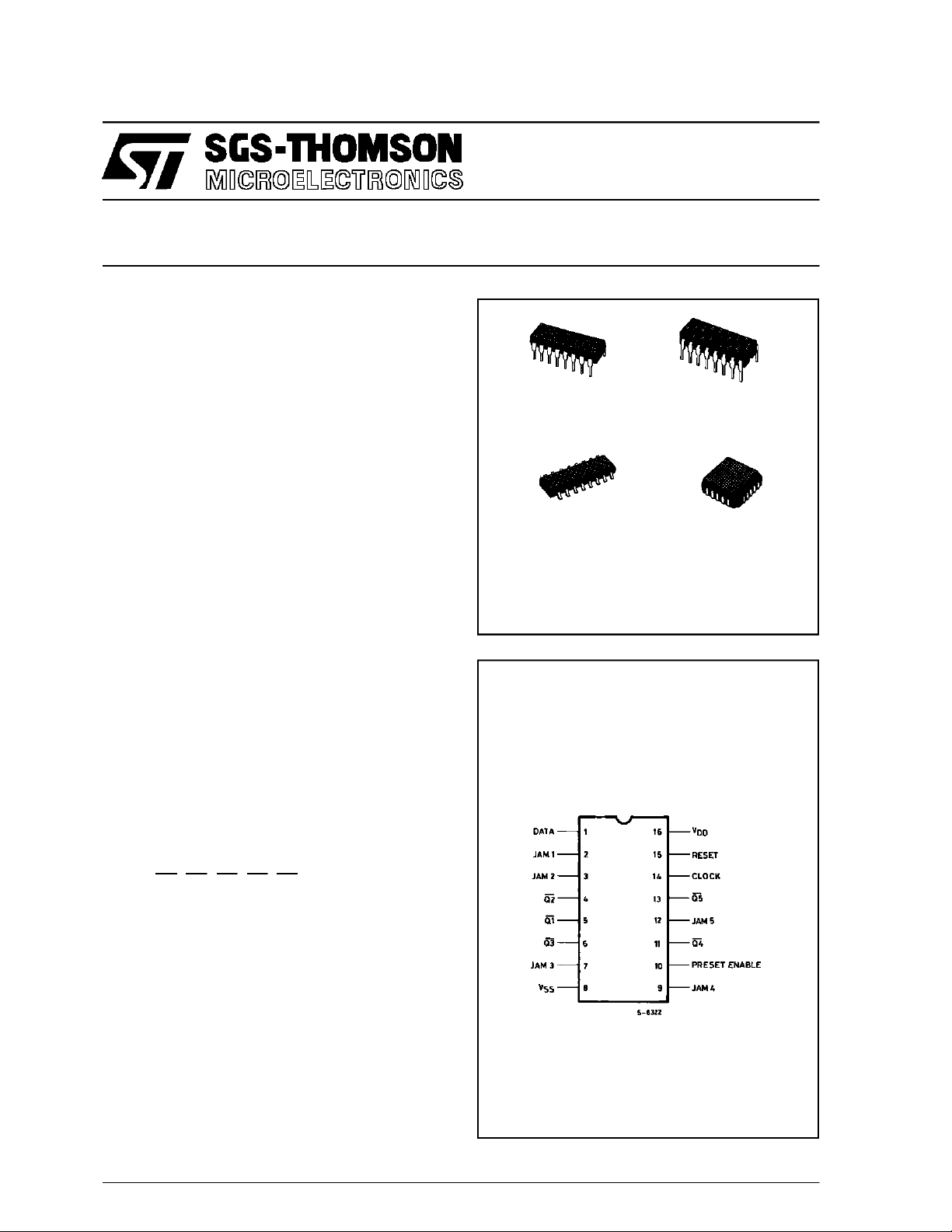
HCC/HCF4018B
EY
(Plastic Package)F(Ceramic FritSealPackage)
M1
(MicroPackage)
ORDERCODES :
HCC4018BF HCF4018BM1
HCF4018BEY HCF4018BC1
(PlasticChip Carrier)
C1
DESCRIPTION
The HCC4018B (extendedtemperature range)and
HCF4018B (intermediate temperature range) are
monolithic integrated circuit, available in 16-lead
dual in-line plastic or ceramic package and plastic
micropackage.
The HCC/HCF4018B types consist of 5 Johnson-
Counter stages, buffered Q outputs from each
stage, and counter preset control gating. CLOCK,
RESET,DATA, PRESETENABLE, and5individual
JAM inputs are provided. Divide by10, 8, 6, 4, or 2
counter configurations canbe implementedbyfeeding the Q5, Q4, Q3, Q2, Q1 signals, respectively,
back to the DATAinput.
Divide-by-9,7,5, or 3 counterconfigurations can be
implemented bythe useof aHCC/HCF4011Bgate
package to properly gate the feedback connection
to the DATA input.Divide-by-functions greaterthan
10 can be achieved by use of multiple HCC/HCF
4018B units. The counterisadvanced onecount at
the positive clock-signal transition. Schmitt Trigger
action on the clock line permits unlimitedclock rise
and fall times. A high RESET signal clears the
counter to an all-zero condition. A highPRESENTENABLE signal allows information on the JAM inputs to preset the counter. Anti-lock gating is
provided to assurethe proper counting sequence.
PIN CO N NECT I ONS
June1989
1/12
HCC/HFC4018B
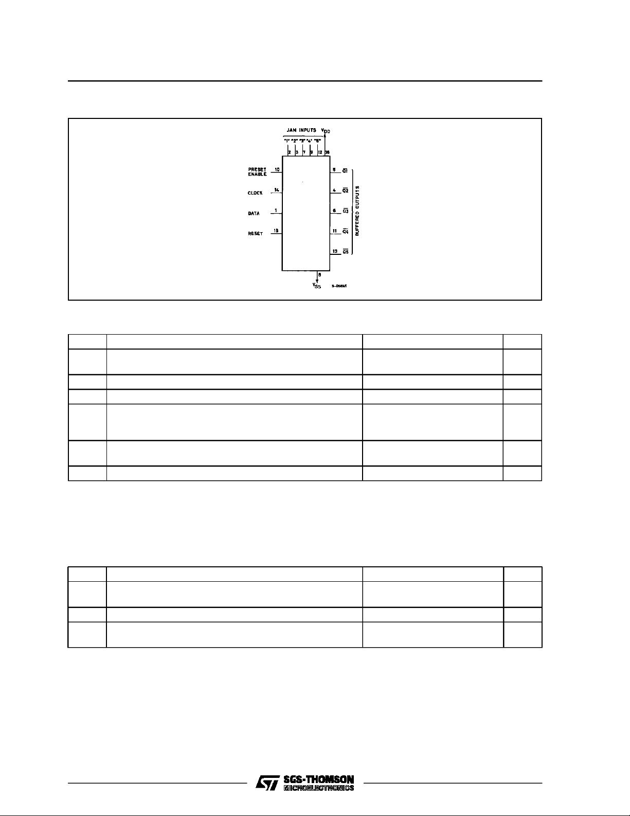
FUNCTIONAL DIAGRAM
ABSOLUTE MAX IMU M RATI NG S
Symbol Parameter Val ue Unit
V
* Supply Voltage : HCC Types
DD
HCF Types
V
Input Voltage – 0.5 to VDD+ 0.5 V
i
I
DC Input Current (any one input) ± 10 mA
I
P
Total Power Dissipation (per package)
tot
Dissipation per Output Transistor
for T
T
Operating Temperature : HCC Types
op
= Full Package-temperature Range
op
HCF Types
T
Stresses above those listed under ”Absolute Maximum Ratings” may cause permanent damage to the device. This is a stress
rating only and functional operation of the device at these or any other conditions above those indicated in the operational sections of this specification is not implied. Exposure to absolute maximum rating conditions for external periods may affect device
reliability.
* All voltage values are refered to VSSpin voltage.
Storage Temperature – 65 to + 150 °C
stg
– 0.5 to + 20
– 0.5 to + 18
200
100
–55to+125
–40to+85
V
V
mW
mW
°C
°C
RECOMMENDED OPERATING C ONDITIONS
Symbol Parameter Value Unit
V
T
2/12
Supply Voltage :HCC Types
DD
HCF Types
V
Input Voltage 0 to V
I
Operating Temperature : HCC Types
op
HCF Types
3to18
3to15
DD
– 55 t o + 125
–40to+85
V
V
V
°C
°C
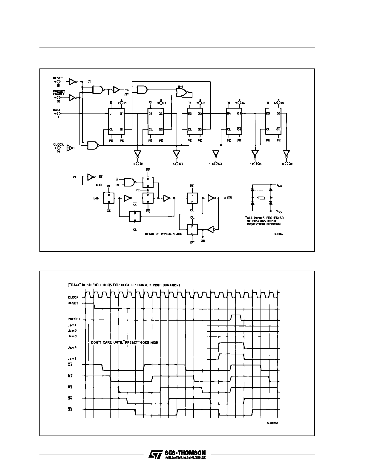
LOGIC DIAGRAM
HCC/HCF4018B
TIMING DIAGRAM
3/12
HCC/HFC4018B
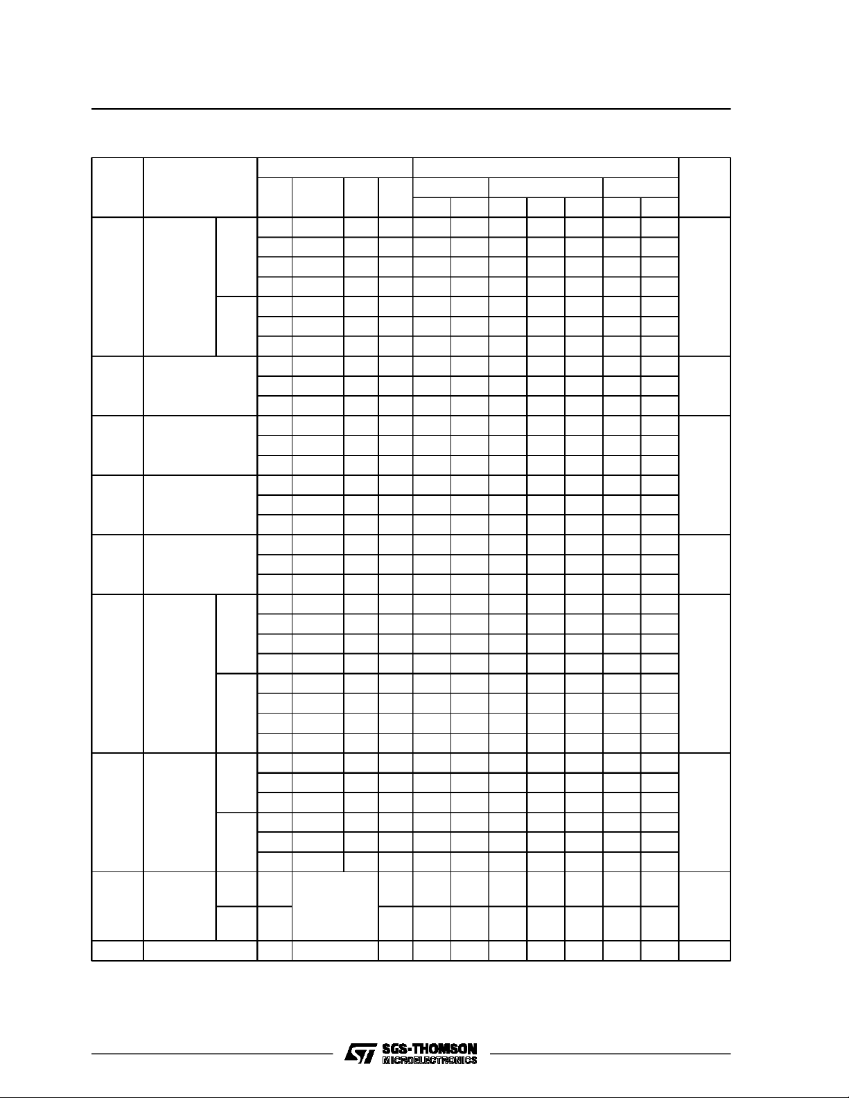
STATIC ELECTRICAL CHARACTERISTICS(under recommendedoperating conditions)
Test Conditions Valu e
Symbol Parameter
(V) (V) (µA) (V)
I
L
Quiescent
Current
HCC
Types
0/ 5 5 5 0.04 5 150
0/10 10 10 0.04 10 300
0/15 15 20 0.04 20 600
0/20 20 100 0.08 100 3000
0/ 5 5 20 0.04 20 150
HCF
Types
0/10 10 40 0.04 40 300
0/15 15 80 0.04 80 600
V
OH
Output High
Voltage
0/ 5 < 1 5 4.95 4.95 4.95
0/10 < 1 10 9.95 9.95 9.95
0/15 < 1 15 14.95 14.95 14.95
V
OL
Output Low
Voltage
5/0 < 1 5 0.05 0.05 0.05
10/0 < 1 10 0.05 0.05 0.05
15/0 < 1 15 0.05 0.05 0.05
V
IH
Input High
Voltage
V
IL
Input Low
Voltage
I
OH
Output
Drive
Current
HCC
Types
0/ 5 2.5 5 – 2 – 1.6 – 3.2 – 1.15
0/ 5 4.6 5 – 0.64 – 0.51 – 1 – 0.36
0/10 9.5 10 – 1.6 – 1.3 – 2.6 – 0.9
0/15 13.5 15 – 4.2 – 3.4 – 6.8 – 2.4
0/ 5 2.5 5 – 1.53 – 1.36 – 3.2 – 1.1
HCF
Types
0/ 5 4.6 5 – 0.52 – 0.44 – 1 – 0.36
0/10 9.5 10 – 1.3 – 1.1 – 2.6 – 0.9
0/15 13.5 15 – 3.6 – 3.0 – 6.8 – 2.4
I
OL
Output
Sink
Current
HCC
Types
0/ 5 0.4 5 0.64 0.51 1 0.36
0/10 0.5 10 1.6 1.3 2.6 0.9
0/15 1.5 15 4.2 3.4 6.8 2.4
0/ 5 0.4 5 0.52 0.44 1 0.36
HCF
Types
0/10 0.5 10 1.3 1.1 2.6 0.9
0/15 1.5 15 3.6 3.0 6.8 2.4
I
IH,IIL
Input
Leakage
Current
HCC
Types
HCF
0/18
0/15 15 ± 0.3 ±10
Types
C
Input Capacitance Any Input 5 7.5 pF
I
*T
=–55°CforHCC device : – 40°CforHCF device.
Low
*T
= +125°CforHCC device : + 85°CforHCF device.
High
The NoiseMargin for both ”1” and”0” levelis : 1V min. withVDD= 5V,2V min.with VDD= 10V, 2.5 V min.withVDD=15V.
V
V
I
O
|IO|V
DD
T
* 25°CT
Low
Min. Max. Min. Typ. Max. Min. Max.
0.5/4.5 < 1 5 3.5 3.5 3.5
1/9 < 1 10 7 7 7
1.5/13.5 < 1 15 11 11 11
4.5/0.5 < 1 5 1.5 1.5 1.5
9/1 < 1 10 3 3 3
13.5/1.5 < 1 15 4 4 4
18 ± 0.1 ±10–5± 0.1 ± 1
Any Input
–5
± 0.3 ± 1
High
Unit
*
µA
V
V
V
V
mA
mA
µA
4/12

HCC/HCF4018B
DYNAMIC ELECTRICAL CHARACTERISTICS (T
=25°C, CL= 50pF, RL= 200kΩ,
amb
typical temperature coefficientfor all VDDvalues is 0.3%/°C, all input rise and fall times = 20ns)
Symbol Parameter
t
PL H,tPHL
t
THL,tTL H
f
CL
t
t
r,tf
t
setup
t
Propagation Delay Time 5 200 400
Transition Time 5 100 200
Maximum Clock Input Frequency 5 3 6
Clock Input Width 5 160 80
W
Clock Input Rise or Fall Time 5
Data Input Set-up Time 5 40 20
Data Input Hold-time 5 140 70
H
PRESET* O R RESET OPERATION
t
PL H,tPHL
Propagation Delay Time
(reset or reset to Q)
t
t
re m
Preset or Reset Pulse Width 5 160 80
W
Preset or Reset Removal Time 5 80 40
Test Conditions
V
(V) Min. Typ. Max.
DD
10 90 180
15 65 130
10 50 100
15 40 80
10 7 14
15 8.5 17
10 70 35
15 50 25
10
15
10 12 6
15 6 3
10 80 40
15 60 30
5 275 550
10 125 250
15 90 180
10 70 35
15 50 25
10 30 15
15 20 10
Value
Unlimited µs
• At PRESET ENABLE OR JAM inputs
Unit
ns
ns
MHz
ns
ns
ns
ns
ns
ns
5/12

HCC/HFC4018B
TypicalOutputLow (sink) Current Characteristics. Typical Output high(source) Current Charac-
teristics.
Minimum Output High (source) Current Characteristics.
typical Output low (sink) Current Characteristics.
6/12

TYPICAL APPLICATIONS
External connections fordivide by 10, 9, 8, 7, 6, 5, 4, 3, 2 operation.
DIVIDEBY 10 Q
DIVIDEBY 8 Q
DIVIDEBY 6 Q
DIVIDEBY 4 Q
DIVIDEBY 2 Q
5
4
3
2
1
CONNECTED
BACKTO
”DATA”
NO CONNECTED
HCC/HCF4018B
NO EXTERNAL
COMPONENTS
REQUIRED
7/12

HCC/HFC4018B
Plastic DIP16 (0.25) MECHANICAL DATA
DIM.
MIN. TYP. MAX. MIN. TYP. MAX.
a1 0.51 0.020
B 0.77 1.65 0.030 0.065
b 0.5 0.020
b1 0.25 0.010
D 20 0.787
E 8.5 0.335
e 2.54 0.100
e3 17.78 0.700
F 7.1 0.280
I 5.1 0.201
L 3.3 0.130
Z 1.27 0.050
mm inch
8/12
P001C

Ceramic DIP16/1 MECHANICAL DATA
HCC/HCF4018B
DIM.
MIN. TYP. MAX. MIN. TYP. MAX.
A 20 0.787
B 7 0.276
D 3.3 0.130
E 0.38 0.015
e3 17.78 0.700
F 2.29 2.79 0.090 0.110
G 0.4 0.55 0.016 0.022
H 1.17 1.52 0.046 0.060
L 0.22 0.31 0.009 0.012
M 0.51 1.27 0.020 0.050
N 10.3 0.406
P 7.8 8.05 0.307 0.317
Q 5.08 0.200
mm inch
P053D
9/12

HCC/HFC4018B
SO16 (Narrow) MECHANICAL DATA
DIM.
MIN. TYP. MAX. MIN. TYP. MAX.
A 1.75 0.068
a1 0.1 0.2 0.004 0.007
a2 1.65 0.064
b 0.35 0.46 0.013 0.018
b1 0.19 0.25 0.007 0.010
C 0.5 0.019
c1 45° (typ.)
D 9.8 10 0.385 0.393
E 5.8 6.2 0.228 0.244
e 1.27 0.050
e3 8.89 0.350
F 3.8 4.0 0.149 0.157
G 4.6 5.3 0.181 0.208
L 0.5 1.27 0.019 0.050
M 0.62 0.024
S8°(max.)
mm inch
10/12
P013H

PLCC20 MECHANICAL DATA
HCC/HCF4018B
DIM.
MIN. TYP. MAX. MIN. TYP. MAX.
A 9.78 10.03 0.385 0.395
B 8.89 9.04 0.350 0.356
D 4.2 4.57 0.165 0.180
d1 2.54 0.100
d2 0.56 0.022
E 7.37 8.38 0.290 0.330
e 1.27 0.050
e3 5.08 0.200
F 0.38 0.015
G 0.101 0.004
M 1.27 0.050
M1 1.14 0.045
mm inch
P027A
11/12

HCC/HFC4018B
Information furnished is believed tobe accurate and reliable. However, SGS-THOMSON Microelectronics assumes no responsability for the
consequences of use of such information nor for any infringementofpatents orother rights of third parties which may results from its use. No
license isgrantedby implication orotherwiseunder any patentorpatent rights ofSGS-THOMSONMicroelectronics. Specificationsmentioned
in this publication are subject to changewithout notice. This publication supersedes and replaces all information previously supplied.
SGS-THOMSON Microelectronicsproductsare notauthorized foruse ascritical componentsin life supportdevices orsystemswithout express
written approval of SGS-THOMSON Microelectonics.
1994 SGS-THOMSON Microelectronics - All RightsReserved
Australia - Brazil - France - Germany - Hong Kong - Italy - Japan - Korea - Malaysia-Malta - Morocco - The Netherlands -
Singapore - Spain - Sweden - Switzerland - Taiwan - Thailand - UnitedKingdom - U.S.A
SGS-THOMSON MicroelectronicsGROUPOF COMPANIES
12/12
 Loading...