

Page 1
LOOK-AHEAD CARRY GENERATOR
.GENERATES HIGH-SPEEDCARRY ACROSS
FOUR ADDERS OFADDER GROUPS
.HIGH-SPEED OPERATIONAL : t
100ns(typ.) @ VDD=10V
PHL=tPLH
.CASCADABLE FOR FAST CARRIES OVER N
BITS
.DESIGNED FOR USE WITHHCC/HCF40181B
ALU
.STANDARDIZED, SYMMETRICAL OUTPUT
CHARACTERISTICS
.QUIESCENT CURRENT SPECIFIED AT 20V
FOR HCC DEVICE
.5V, 10V,AND 15VPARAMETRIC RATINGS
.INPUT CURRENT OF 100nA AT18V AND25°C
FOR HCC DEVICE
.100% TESTEDFOR QUIESCENTCURRENT
.MEETSALLREQUIREMENTSOFJEDECTEN-
TATIVESTANDARDN°13A,”STANDARDSPECIFICATIONS FOR DESCRIPTION OF ”B”
SERIESCMOS DEVICES”
HCC/H CF4 01 82B
=
EY
(Plastic Package)F(CeramicFritSeal Package)
M1
(MicroPackage)
ORDER CODES :
HCC40182BFHCF4018
2BM1
(PlasticChip Carrier)
C1
DESCRIPTI ON
The HCC40182B (extended temperature range)
and HCF40182B (intermediate temperature range)
are monolithic integrated circuits, available in 16lead dual in-line plastic or ceramic package and
plastic micro package. The HCC/HCF40182B is a
high-speed look-ahead carry generator capable of
anticipating a carry across four binary adders or
groupsofadders. TheHCC/HCF40182B is cascad-
able toperform full look-ahead acrossn-bit adders.
Carry, propagate-carry, and generate-carry functions are provided as enumerated in the terminal
designation below. The HCC/HCF40182B, when
used in conjunction with the HCC/HCF40181B
arithmetic logic unit (ALU), provides fullhigh-speed
look-ahead carry capability for up to n-bit words.
Each HCC/HCF40182B generatesthe look-ahead
(anticipated carry) across a group of four ALU’s.In
addition, other HCC/HCF40182B’s may be em-
playedtoanticipate the carry across sections of four
look-ahead blocksup ton-bits. Carryinputsand outputs ofthe HCC/HCF40181B are active-high logic,
andcarry-generate(G)andcarry-propagate (P)outputsareactivelow.Thereforetheinputsandoutputs
of the HCC/HCF40182B are compatible. The
HCC/HCF40182B is similar to industry type
MC14582.
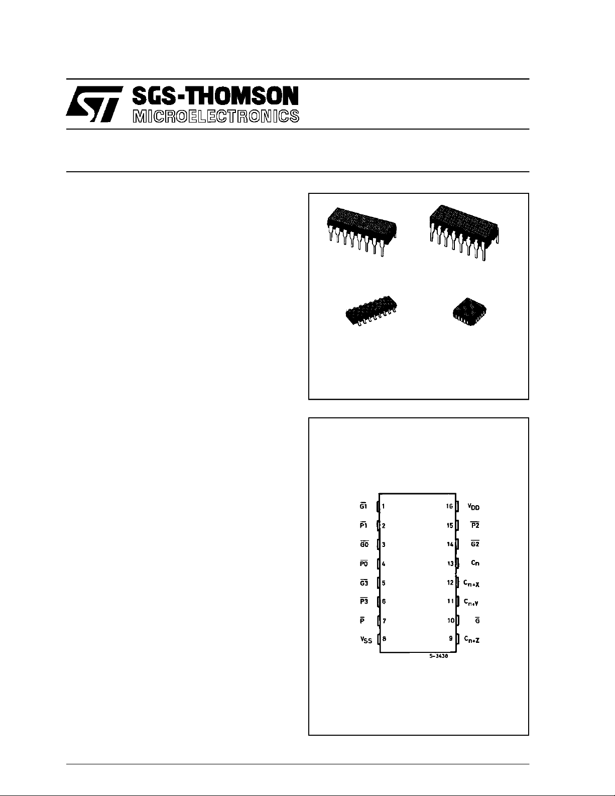
PIN CONNECTIONS
June1989
1/12
Page 2
HCC/HCF40182B
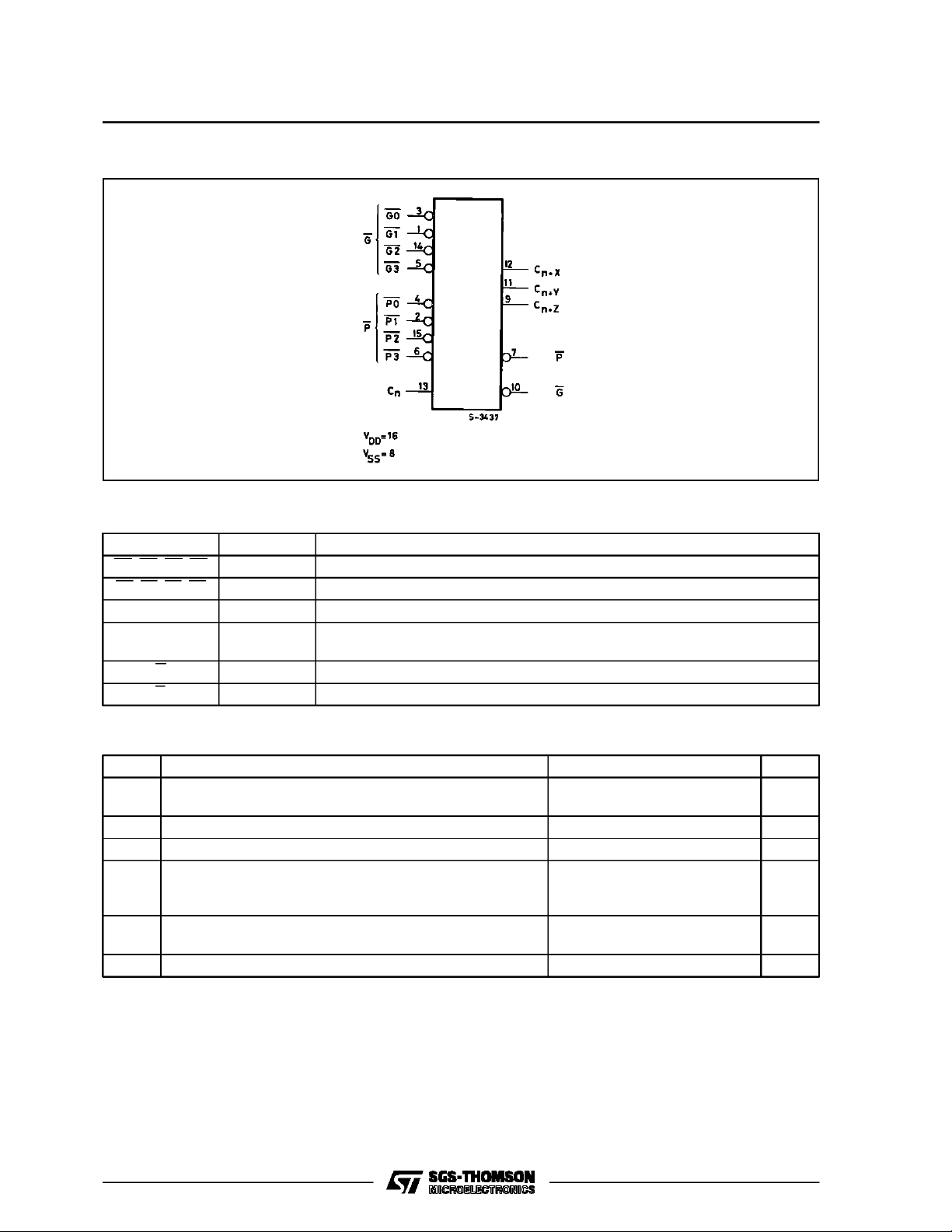
FUN CTIONAL DIAG R A M
TERMINAL DESIGNATIONS TABLE
Pin Name Pin Function
G0,G1, G2,G3 3, 1, 14, 5 Active-low Carry-generate Inputs
P0, P1, P2,P3 4, 2, 15, 6 Active-low Carry-propagate Inputs
C
n
C
n+X,Cn+Y
C
,
n+Z
G 10 Active-low Group Carry-generate Output
P 7 Active-low Group Carry-propagate Output
13 Active-high Carry Input
12, 11, 9 Active-high Carry Outputs
ABSOLUTE M AXI MUM RATIN GS
Symbol Parameter Value Unit
V
* Supply Voltage :HC C Types
DD
HCF Types
V
Input Voltage – 0.5 to VDD+ 0.5 V
i
I
DC Input Current (any one input) ± 10 mA
I
P
Total Power Dissipation (per package)
tot
Dissipation per Output Transistor
for T
T
Operating Temperature : HCC Types
op
= Full Package-temperature Range
op
HCF Types
T
Stresses above those listed under ”Absolute Maximum Ratings” may cause permanent damage to the device. This is a stress
rating only and functional operation of the device at these or any other conditions above those indicated in the operational sections
of this specification is not implied. Exposure to absolute maximum rating conditions for external periods may affect device reliability.
* All voltages are with respect to VSS(GND).
Storage Temperature – 65 to + 150 °C
stg
2/12
– 0.5 to + 20
– 0.5 to + 18
200
100
– 55 to + 125
–40to+85
V
V
mW
mW
°C
°C
Page 3
HCC/HCF40182B
RECOMMENDED OPERATING CO NDITIONS
Symbol Parameter Value Unit
V
T
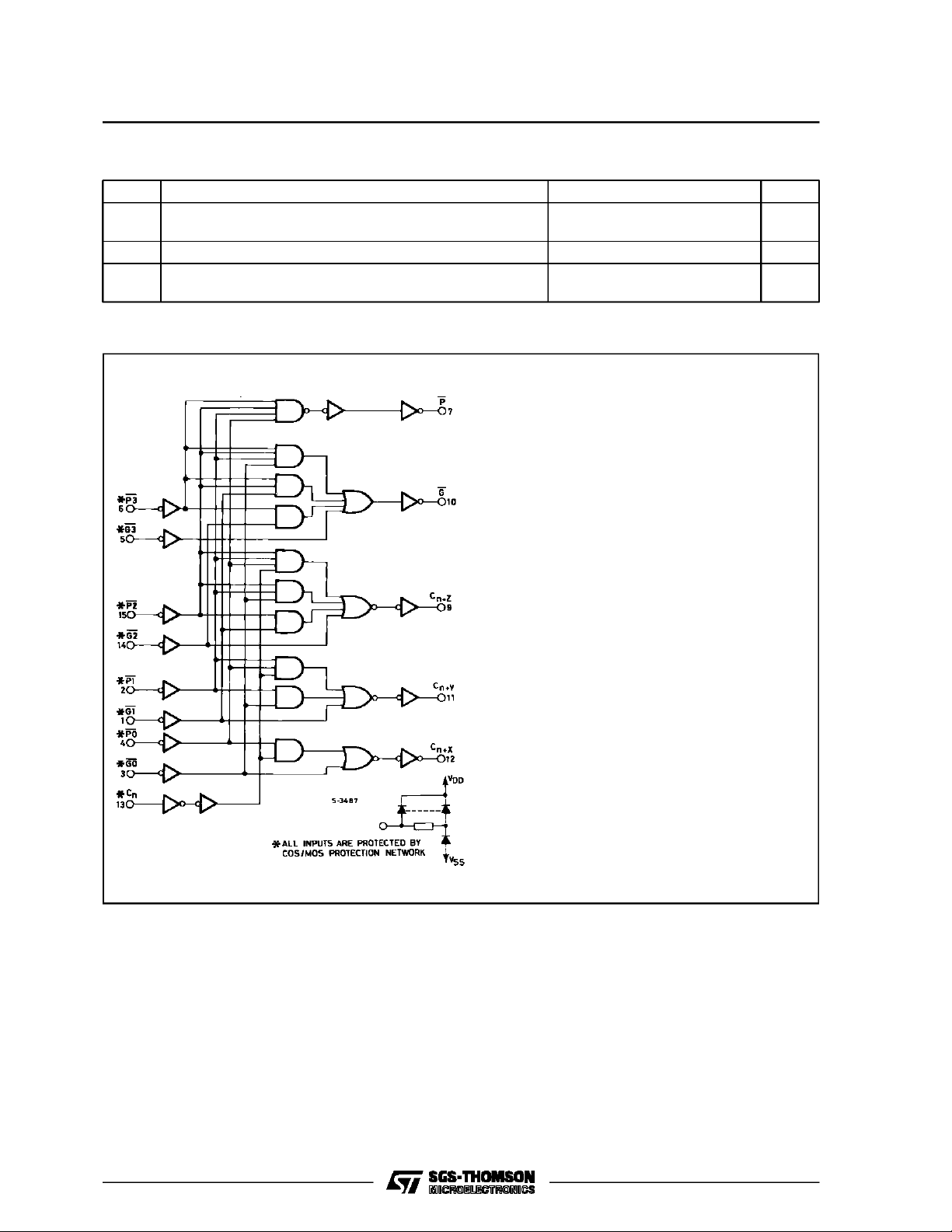
LOGI C DI AG RAM
Supply Voltage : HCC Types
DD
V
Input Voltage 0 to V
I
Operating Temperature : HCC Types
op
HCF Types
HCF Types
LogicEquations :
C
=G0+P0•Cn
n+X
3to18
3to15
DD
– 55 to + 125
–40to+85
V
V
V
°C
°C
C
n+Y
=G1+P1•G0 + P1 • P0 • C
n
3/12
Page 4
HCC/HCF40182B
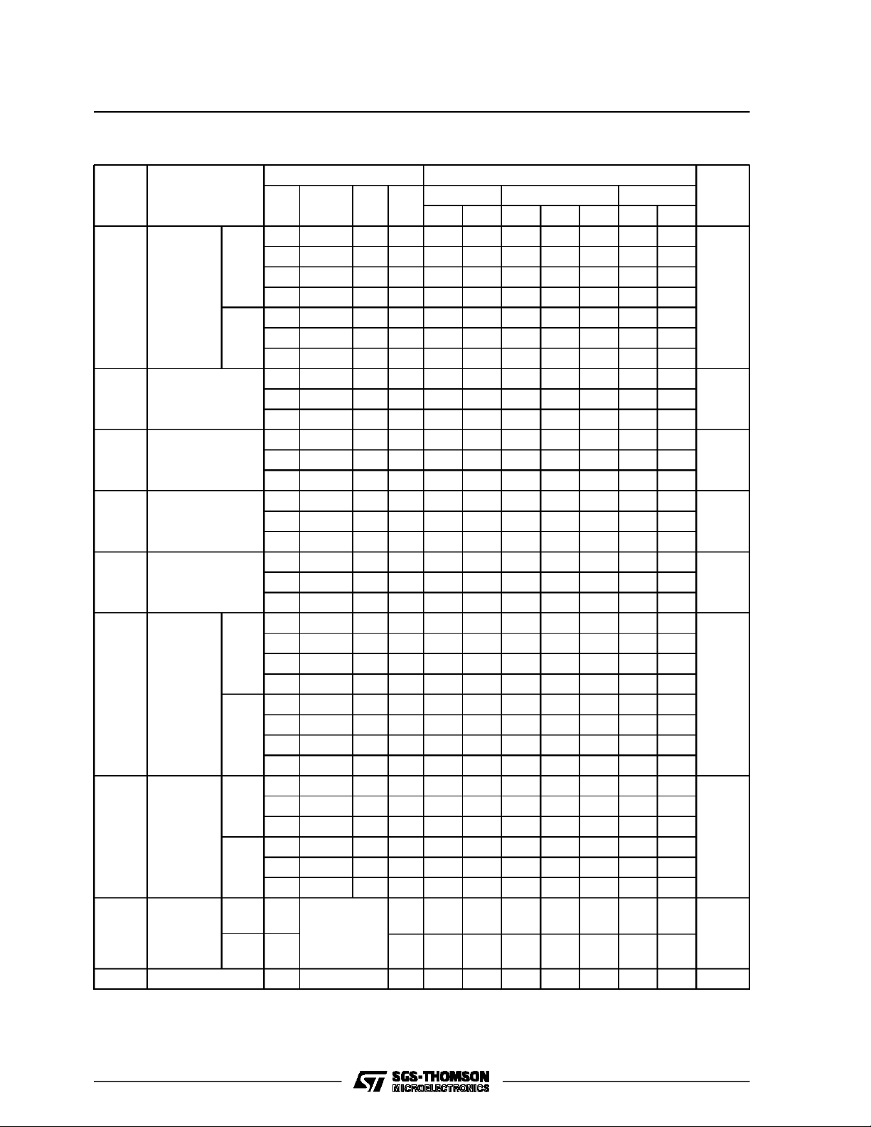
STATIC ELECTRICAL CHARACTERISTICS(over recommended operating conditions)
Test Conditions Value
Symbol Parameter
I
Quiescent
L
Current
HCC
Types
HCF
Types
V
OH
Output High
Voltage
V
OL
Output Low
Voltage
V
IH
Input High
Voltage
IL
Input Low
V
Voltage
I
OH
Output
Drive
Current
HCC
Types
HCF
Types
I
OL
Output
Sink
Current
HCC
Types
HCF
Types
I
IH,IIL
Input
Leakage
Current
HCC
Types
HCF
Types
Input Capacitance Any Input 5 7.5 pF
C
I
*T
=–55°CforHCC device : – 40°CforHCF device.
Low
*T
= + 125°C for HCC device : + 85°C for HCF device.
High
V
V
I
(V) (V) (µA) (V)
O
|IO|V
DD
T
* 25°CT
Low
Min. Max. Min. Typ. Max. Min. Max.
0/ 5 5 5 0.04 5 150
0/10 10 10 0.04 10 300
0/15 15 20 0.04 20 600
0/20 20 100 0.08 100 3000
0/ 5 5 20 0.04 20 150
0/10 10 40 0.04 40 300
0/15 15 80 0.04 80 600
0/ 5 < 1 5 4.95 4.95 5 4.95
0/10 < 1 10 9.95 9.95 10 9.95
0/15 < 1 15 14.95 14.95 15 14.95
5/0 < 1 5 0.05 0.05 0.05
10/0 < 1 10 0.05 0.05 0.05
15/0 < 1 15 0.05 0.05 0.05
0.5/4.5 < 1 5 3.5 3.5 3.5
1/9 < 1 10 7 7 7
1.5/13.5 < 1 15 11 11 11
4.5/0.5 < 1 5 1.5 1.5 1.5
9/1 < 1 10 3 3 3
13.5/1.5 < 1 15 4 4 4
0/ 5 2.5 5 – 2 – 1.6 – 3.2 – 1.15
0/ 5 4.6 5 – 0.64 – 0.51 – 1 – 0.36
0/10 9.5 10 – 1.6 – 1.3 – 2.6 – 0.9
0/15 13.5 15 – 4.2 – 3.4 – 6.8 – 2.4
0/ 5 2.5 5 – 1.53 – 1.36 – 3.2 – 1.1
0/ 5 4.6 5 – 0.52 – 0.44 – 1 – 0.36
0/10 9.5 10 – 1.3 – 1.1 – 2.6 – 0.9
0/15 13.5 15 – 3.6 – 3.0 – 6.8 – 2.4
0/ 5 0.4 5 0.64 0.51 1 0.36
0/10 0.5 10 1.6 1.3 2.6 0.9
0/15 1.5 15 4.2 3.4 6.8 2.4
0/ 5 0.4 5 0.52 0.44 1 0.36
0/10 0.5 10 1.3 1.1 2.6 0.9
0/15 1.5 15 3.6 3.0 6.8 2.4
0/18
18 ± 0.1 ±10
–5
± 0.1 ± 1
Any Input
0/15
15 ± 0.3 ±10
–5
± 0.3 ± 1
High
Unit
*
µA
V
V
V
V
mA
mA
µA
4/12
Page 5
HCC/HCF40182B
DYNAMIC ELECTRICAL CHARACTERISTICS(T
=25°C, CL= 50pF, RL= 200kΩ,
amb
typical temperature coefficient for all VDDvalues is 0.3%/°C, all input rise and fall time = 20ns)
Symbol Parameter
t
t
PHL
PLH
Propagation Delay Time
,
P, G, into P
G Out and Carry Outs
to Carry Outs 5 240 480
C
n
t
t
TLH
THL
Transition Time 5 100 200
,
Test Conditions Value
(V) Min. Typ. Max.
V
DD
5 200 400
10 100 200
15 75 150
10 120 240
15 90 180
10 50 100
15 40 80
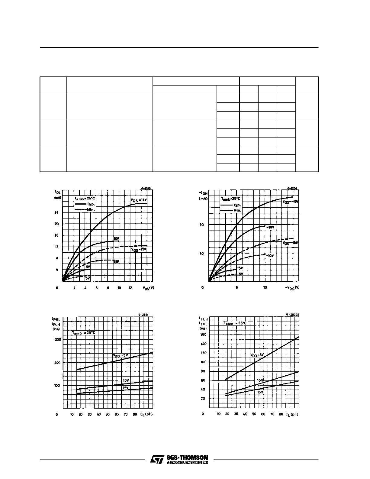
OutputLow (sink) Current Characteristics. OutputHigh (source)Current Characteristics.
Unit
ns
ns
ns
TypicalPropagation Delay Time (P, G In to P, G
Out andCarry-outs) vs.Load Capacitance.
TypicalTransition Time vs. Load Capacitance.
5/12
Page 6
HCC/HCF40182B
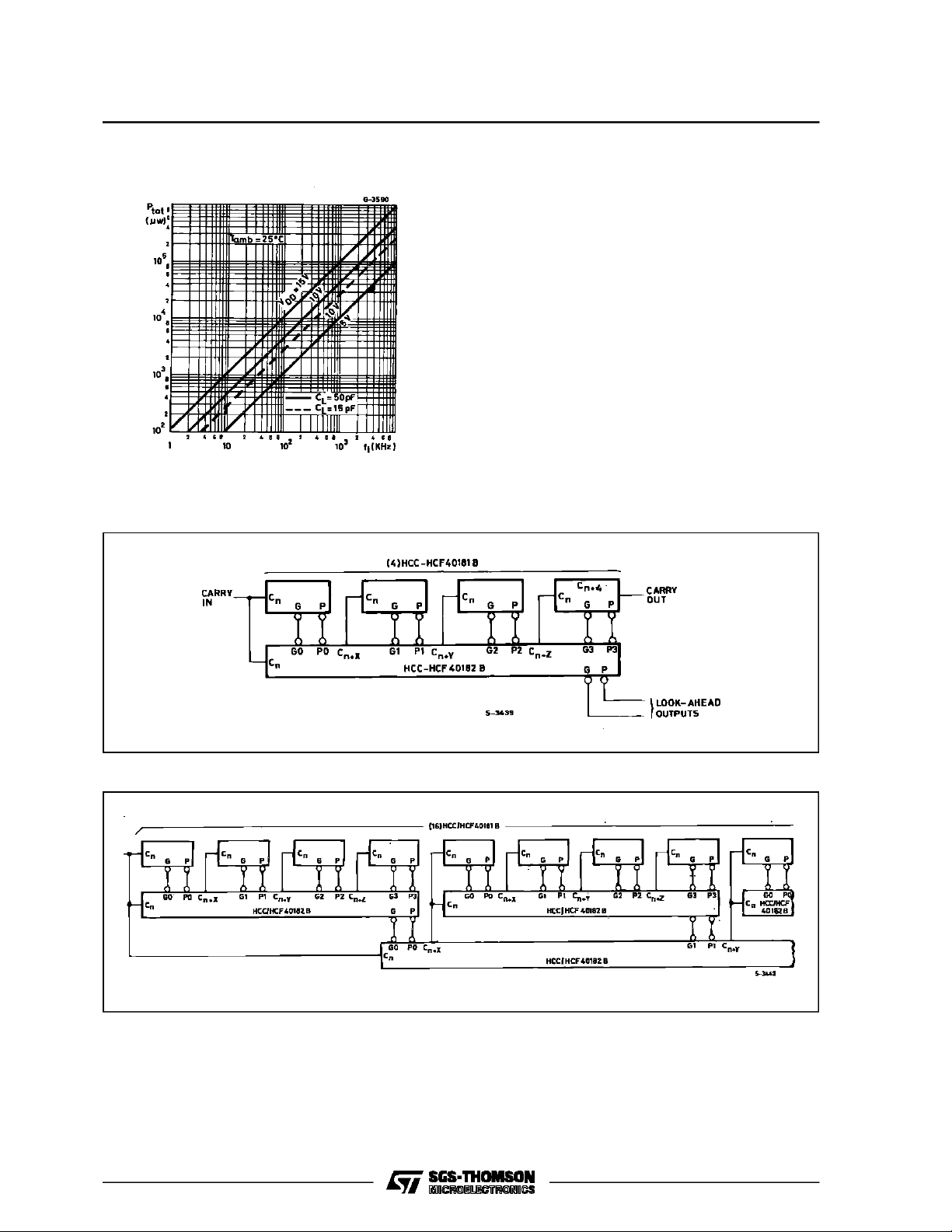
TypicalDynamicPower Dissipation vs. Input Frequency.
TYPICAL APPLICA TI O NS
16-BITTWO-LEVELLOOK-AHEADALU
64-BITFULL CARRYLOOK-AHEAD ALU IN 3LEVELS
6/12
Page 7
TYPICAL APPLICA TI O NS (c ontinued)
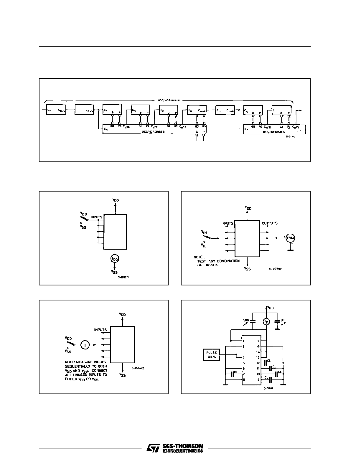
COMBINEDTWO-LEVEL LOOK-AHEAD AND RIPPLE-CARRY ALU
TEST CIRCUITS
QuiescentDevice Current. Input Voltage.
HCC/HCF40182B
Input Leakage Current. DynamicPower Dissipation.
7/12
Page 8

HCC/HCF40182B
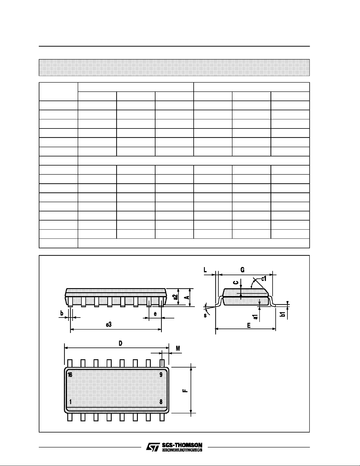
Plastic DIP16 (0.25) MECHANICAL DATA
DIM.
MIN. TYP. MAX. MIN. TYP. MAX.
a1 0.51 0.020
B 0.77 1.65 0.030 0.065
b 0.5 0.020
b1 0.25 0.010
D 20 0.787
E 8.5 0.335
e 2.54 0.100
e3 17.78 0.700
F 7.1 0.280
I 5.1 0.201
L 3.3 0.130
Z 1.27 0.050
mm inch
8/12
P001C
Page 9

Ceramic DIP16/1 MECHANICAL DATA
HCC/HCF40182B
DIM.
MIN. TYP. MAX. MIN. TYP. MAX.
A 20 0.787
B 7 0.276
D 3.3 0.130
E 0.38 0.015
e3 17.78 0.700
F 2.29 2.79 0.090 0.110
G 0.4 0.55 0.016 0.022
H 1.17 1.52 0.046 0.060
L 0.22 0.31 0.009 0.012
M 0.51 1.27 0.020 0.050
N 10.3 0.406
P 7.8 8.05 0.307 0.317
Q 5.08 0.200
mm inch
P053D
9/12
Page 10
HCC/HCF40182B
SO16 (Narrow) MECHANICAL DATA
DIM.
MIN. TYP. MAX. MIN. TYP. MAX.
A 1.75 0.068
a1 0.1 0.2 0.004 0.007
a2 1.65 0.064
b 0.35 0.46 0.013 0.018
b1 0.19 0.25 0.007 0.010
C 0.5 0.019
c1 45° (typ.)
D 9.8 10 0.385 0.393
E 5.8 6.2 0.228 0.244
e 1.27 0.050
e3 8.89 0.350
F 3.8 4.0 0.149 0.157
G 4.6 5.3 0.181 0.208
L 0.5 1.27 0.019 0.050
M 0.62 0.024
S8°(max.)
mm inch
10/12
P013H
Page 11
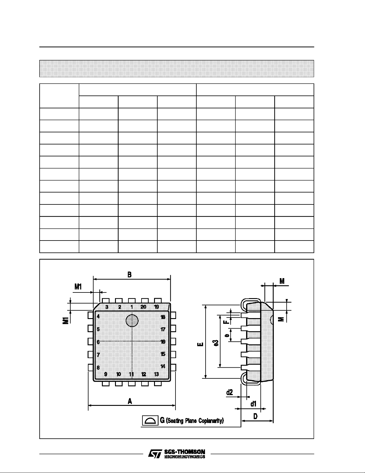
PLCC20 MECHANICAL DATA
HCC/HCF40182B
DIM.
MIN. TYP. MAX. MIN. TYP. MAX.
A 9.78 10.03 0.385 0.395
B 8.89 9.04 0.350 0.356
D 4.2 4.57 0.165 0.180
d1 2.54 0.100
d2 0.56 0.022
E 7.37 8.38 0.290 0.330
e 1.27 0.050
e3 5.08 0.200
F 0.38 0.015
G 0.101 0.004
M 1.27 0.050
M1 1.14 0.045
mm inch
P027A
11/12
Page 12

HCC/HCF40182B
Information furnished isbelieved tobe accurateand reliable.However, SGS-THOMSONMicroelectronics assumes no responsability for the
consequences of use of suchinformation nor for any infringementof patents or other rightsof thirdparties which mayresults fromits use. No
license is granted by implication or otherwise underany patent or patent rights of SGS-THOMSON Microelectronics. Specificationsmentioned
in this publicationare subject to changewithout notice.This publication supersedes andreplaces all information previously supplied.
SGS-THOMSON Microelectronicsproductsare notauthorized for use ascritical componentsin life supportdevices orsystems without express
written approval of SGS-THOMSON Microelectonics.
1994SGS-THOMSON Microelectronics - All RightsReserved
Australia - Brazil - France- Germany - Hong Kong - Italy - Japan - Korea - Malaysia - Malta -Morocco -The Netherlands-
Singapore - Spain - Sweden- Switzerland- Taiwan -Thailand - UnitedKingdom -U.S.A
SGS-THOMSON Microelectronics GROUP OF COMPANIES
12/12
 Loading...