

Page 1
.FULL LOOK-AHEAD CARRY FOR SPEED
OPERATIONSON LONG WORDS
.GENERATES 16 LOGICFUNCTIONSOFTWO
BOOLEANVARIABLES
.GENERATES 16 ARITHMETIC FUNCTIONS
OF TWO 4-BIT BINARY WORDS
.A =B COMPARATOR OUTPUT AVAILABLE
.RIPPLE-CARRY INPUT AND OUTPUT AVAIL-
ABLE
.TYPICALADDITION TIME 200ns @ V
DD
= 10V
.STANDARDIZED SYMMETRICAL OUTPUT
CHARACTERISTICS
.QUIESCENTCURRENTAT20VFORHCCDE-
VICE
.5V, 10V, AND 15V PARAMETRIC RATINGS
.INPUT CURRENTOF100nA AT 18V AND25°C
FOR HCC DEVICE
.100% TESTEDFOR QUIESCENTCURRENT
.MEETSALLREQUIREMENTSOFJEDECTEN-
TATIVESTANDARDN°13A,”STANDARD SPECIFICATIONS FOR DESCRIPTION OF ”B”
SERIESCMOS DEVICES”
HCC/H CF4 01 81B
4-BIT ARITHMETIC LOGIC UNIT
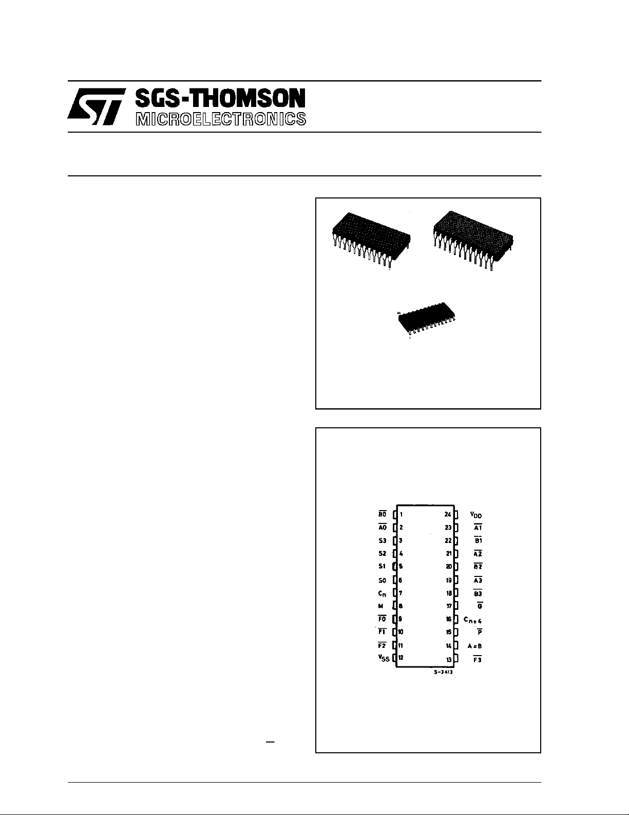
EY
(Plastic Package)F(CeramicFrit Seal Package)
M1
(MicroPackage)
ORDER CODES :
HCC40181BF HCF40181BEY
HCF40181BM1
PIN CONNECTIONS
DESCRIPTI ON
The HCC40181B (extended temperature range)
and HCF40181B (intermediate temperaturerange)
are monolithic integrated circuits, available in 24lead dual in-line plastic or ceramic package and
plastic micro package. The HCC/HCF40181B is a
low-power four-bit parallel arithmetic logic unit
(ALU) capable of providing 16 binary arithmetic
operations ontwo four-bitwords and16logical functions of two Boolean variables. The mode control
inputM selectslogical(M =High) orarithmetic (M=
Low)operation. The four select inputs (S0, S1, S2,
and S3)selectthedesired logical orarithmeticfunctions,whichincludeAND,OR,NAND,NOR,andexclusive-OR and-NOR in the logical mode, and
addition, subtraction, decrement, left-shift and
straighttransferinthe arithmeticmode,accordingto
the truth table. The HCC/HCF40181B operation
may be interpreted with either active-low or activehighdataattheAandBwordinputs and thefunction
outputs F, by usingthe appropriate truth table. The
HCC/HCF40181B containslogicfor full look-ahead
carry operation for fast carry generation using the
carry-generate and carry-propagate outputs G and
June1989
1/12
Page 2
HCC/HCF40181B
P for the four bits of the HCC/HCF40181B. Use of
the HCC/HCF40182B look-ahead carry generator
inconjunctionwithmultiple HCC/HCF40181B’sper-
mits high-speed arithmetic operations on long
words. Aripple carryoutput C
isavailable foruse
n+4
in systems where speed is not of primary importance. Also included in the HCC/HCF40181B is a
comparator output A = B, which assumes a high
level whenever the twofour-bit input words A andB
are equal and thedevice is in the subtractmode. In
addition, relative magnitude information may be
derived from the carry-ininput Cnandripple carryout output C
n+4
modeandexternally decoding usingthe information
in tableII. TheHCC/HCF40181B issimilar to indus-
try types MC 14581 and74181.
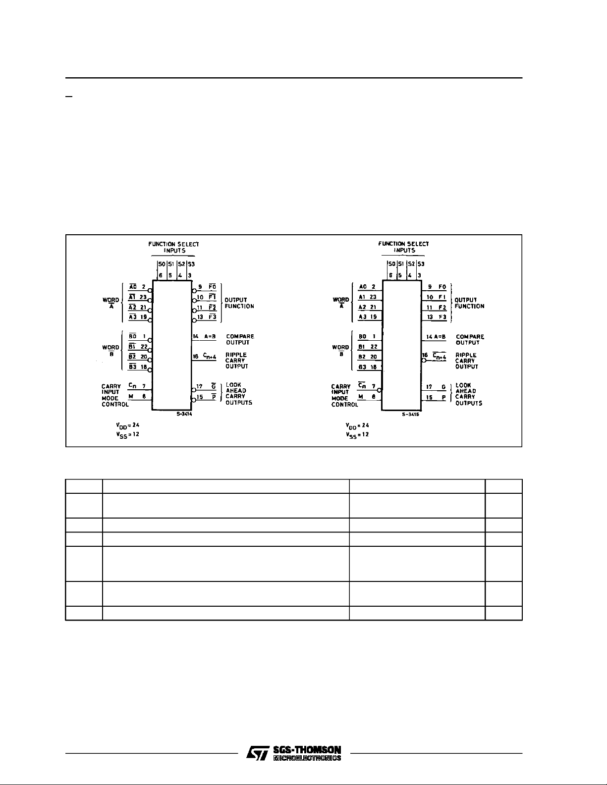
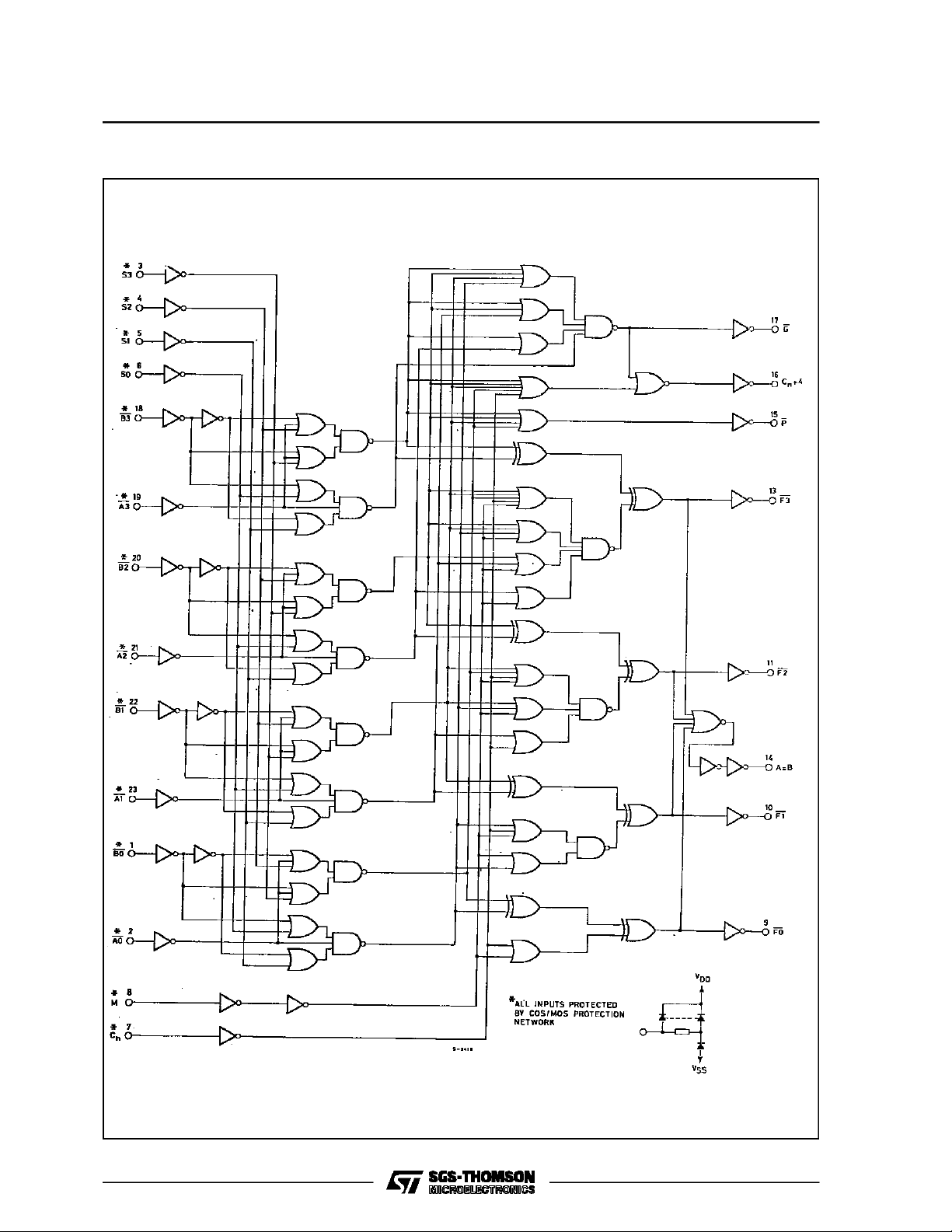
FUN CTIONAL DI AG R A M
Active-low Data. Active-highData.
by placing the unit in the subtract
ABSOLUTE MAXI MUM RAT INGS
Symbol Parameter Value Unit
V
* Supply Voltage :HC C Types
DD
V
Input Voltage – 0.5 to VDD+ 0.5 V
i
I
DC Input Current (any one input) ± 10 mA
I
P
T
T
Stresses above those listed under ”Absolute Maximum Ratings” may cause permanent damage to the device. This is a stress
rating only and functional operation of the device at these or any other conditions above those indicated in the operational sections
of this specification is not implied. Exposure to absolute maximum rating conditions for external periods may affect device reliability.
* All voltages are with respect to VSS(GND).
2/12
Total Power Dissipation (per packa ge)
tot
Dissipation per Output Transistor
for Top= Full Package-temperature Range
Operating Temperature : HCC Types
op
Storage Temperature – 65 to + 150 °C
stg
HCF Types
HCF Types
– 0.5 to + 20
– 0.5 to + 18
200
100
– 55 t o + 125
–40to+85
V
V
mW
mW
°C
°C
Page 3
HCC/HCF40181B
RECOMMENDED OPERATING CO NDITIONS
Symbol Parameter Value Unit
V
T
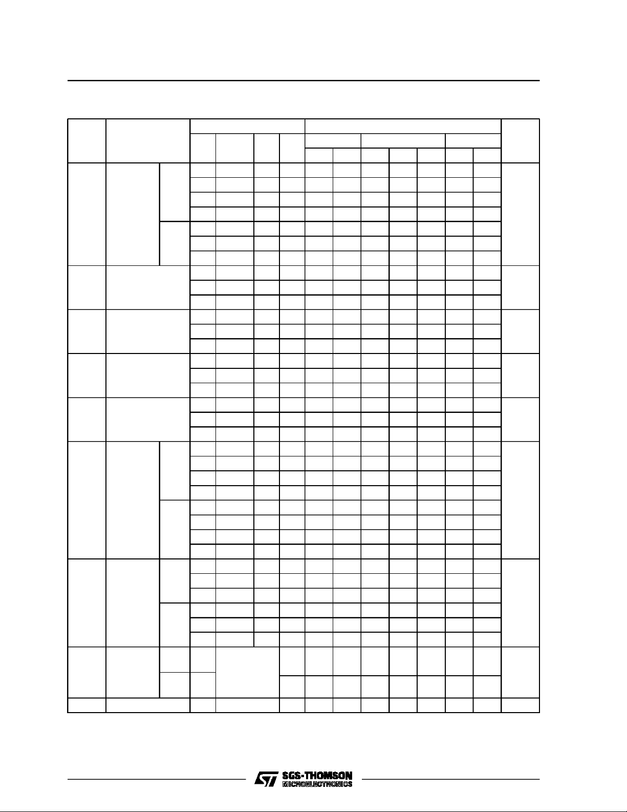
TRUTH TABLES
Table 1.
Supply Voltage : HCC Types
DD
HCF Types
V
Input Voltage 0 to V
I
Operating Temperature : HCC Types
op
HCF Types
3to18
3to15
DD
– 55 t o + 125
–40to+85
V
V
V
°C
°C
Function
Select
S3 S2 S1 S0
Inputs/OutputsActive Low Inputs/Outputs Active High
Logic
Function
(M= H)
Arithmetic*
Function
(M = L, C
n
=L)
Logic
Function
(M= H)
Arithmetic*
Function
(M = L, Cn=H)
0 0 0 0 A A minus 1 A A
0 0 0 1 AB AB minus 1 A+ B A + B
0010 A+B ABminus1 AB A+B
0 0 1 1 Logic 1 minus 1 Logic 0 minus 1
0 1 0 0 A+ B A plus (A + B) AB A plus AB
0 1 0 1 B AB plus (A + B) B (A + B) plus AB
0110 AB
⊕
A minus B minus 1 A ⊕ B A minus B minus 1
0 1 1 1 A + B A + B AB AB minus 1
1 0 0 0 AB A plus (A + B) A + B A plus AB
1001 A⊕B A plus B A B
⊕
A plus B
1 0 1 0 B AB plus (A + B) B (A + B) plus AB
1 0 1 1 A + B A + B AB AB minus 1
1 1 0 0 Logic 0 A plus A Logic 1 A plus A
1 1 0 1 AB AB plus A A + B (A + B) plus A
1 1 1 0 AB AB plus A A + B (A + B) plus A
1111 A A A Aminus1
* Expressed as two’s complement. For arithmetic function with Cnin the opposite state, the resulting function is as show plus 1.
1 = HIGH LEVEL.
0 = LOW LEVEL.
Table 2 : Magnitude Comparison.
Active-high Data Active-l ow Data
Input
C
n
11 A≤B00A≤B
01 A<B 10 A<B
10 A>B 01 A>B
00 A≥B11A≥B
1 = HIGH LEVEL
0 = LOW LEVEL
Output
C
n+4
Magnitude
Input
C
n
Output
C
n+4
Magnitude
3/12
Page 4
HCC/HCF40181B
LOGI C DIAG RAM Activ e-low D ata
4/12
Page 5
HCC/HCF40181B
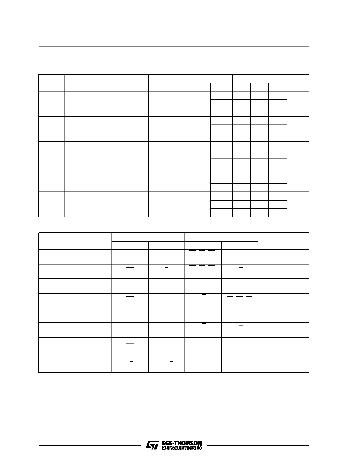
STATIC ELECTRICAL CHARACTERISTICS (over recommended operating conditions)
Test Conditions Value
Symbol P arameter
I
Quiescent
L
Current
HCC
Types
HCF
Types
V
OH
Output High
Voltage
V
OL
Output Low
Voltage
V
IH
Input High
Voltage
IL
Input Low
V
Voltage
I
OH
Output
Drive
Current
HCC
Types
HCF
Types
I
OL
Output
Sink
Current
HCC
Types
HCF
Types
I
IH,IIL
Input
Leakage
Current
HCC
Types
HCF
Types
C
Input Capacitance Any Input 5 7.5 pF
I
*T
=–55°CforHCC device : – 40°CforHCF device.
Low
*T
= + 125°CforHCC device : + 85°CforHCF device.
High
The Noise Margin for both ”1” and ”0” level is : 1V min. with VDD= 5V, 2V min. with VDD= 10V, 2.5V min. with VDD= 15V.
V
V
I
(V) (V) (µA) (V)
O
|IO|V
T
DD
* 25°CT
Low
Min. Max. Min. Typ. Max. Min. Max.
High
*
0/ 5 5 5 0.04 5 150
0/10 10 10 0.04 10 300
0/15 15 20 0.04 20 600
0/20 20 100 0.08 100 3000
0/ 5 5 20 0.04 20 150
0/10 10 40 0.04 40 300
0/15 15 80 0.04 80 600
0/ 5 < 1 5 4.95 4.95 4.95
0/10 < 1 10 9.95 9.95 9.95
0/15 < 1 15 14.95 14.95 14.95
5/0 < 1 5 0.05 0.05 0.05
10/0 < 1 10 0.05 0.05 0.05
15/0 < 1 15 0.05 0.05 0.05
0.5/4.5 < 1 5 3.5 3.5 3.5
1/9 < 1 10 7 7 7
1.5/13.5 < 1 15 11 11 11
4.5/0.5 < 1 5 1.5 1.5 1.5
9/1 < 1 10 3 3 3
13.5/1.5 < 1 15 4 4 4
0/ 5 2.5 5 – 2 – 1.6 – 3.2 – 1.15
0/ 5 4.6 5 – 0.64 – 0.51 – 1 – 0.36
0/10 9.5 10 – 1.6 – 1.3 – 2.6 – 0.9
0/15 13.5 15 – 4.2 – 3.4 – 6.8 – 2.4
0/ 5 2.5 5 – 1.53 – 1.36 – 3.2 – 1.1
0/ 5 4.6 5 – 0.52 – 0.44 – 1 – 0.36
0/10 9.5 10 – 1.3 – 1.1 – 2.6 – 0.9
0/15 13.5 15 – 3.6 – 3.0 – 6.8 – 2.4
0/ 5 0.4 5 0.64 0.51 1 0.36
0/10 0.5 10 1.6 1.3 2.6 0.9
0/15 1.5 15 4.2 3.4 6.8 2.4
0/ 5 0.4 5 0.52 0.44 1 0.36
0/10 0.5 10 1.3 1.1 2.6 0.9
0/15 1.5 15 3.6 3.0 6.8 2.4
0/18
0/15
Any Input
18 ± 0.1 ±10
15 ± 0.3 ±10
–5
± 0.1 ± 1
–5
± 0.3 ± 1
Unit
µA
V
V
V
V
mA
mA
µA
5/12
Page 6
HCC/HCF40181B
DYNAMIC ELECTRICAL CHARACTERISTICS (T
=25°C, CL= 50pF, RL= 200kΩ,
amb
typical temperature coefficient for all VDDvalues is 0.3%/°C, all input rise and fall time = 20ns)
Symbol Parameter
t
,
Propagation Delay Time
A or B to F (logic mode)
t
PLH
PHL
AorBtoGorP
AorBtoF,
C
,orA=B
n+4
C
to F 5 320 640
n
to C
C
n
n+4
t
,
Transition Time 5 100 200
t
TLH
THL
Test Conditions Value
(V) Min. Typ. M ax.
V
DD
5400800
10 160 320
15 120 240
5 300 1000
10 200 400
15 140 280
10 135 270
15 100 200
5200400
10 100 200
15 70 140
10 50 100
15 40 80
Table 3 : AC Test Setup Reference (active-low data).
Unit
ns
ns
ns
ns
ns
Test
Delay T imes
to SUM
SUM
IN
SUM
to P AO P
IN
SUM
to G BO G
IN
SUM
to C
IN
to SUM
C
n
C
to C
n
OUT
n+4
OUT
n+4
AC Paths DC D ata Inputs
Inputs Outputs to V
BO Any F
SS
B1, B2, B3,
M, C
n
A1, A2, A3,
M, C
n
All A’s
M, C
n
BO C
C
n
C
n
n+4
Any F
C
n+4
All A’s,
M, C
All A’s,
M
All A’s,
M
n
to V
All A’s ADD
All B’s ADD
B1, B2, B3 ADD
B1, B2, B3 ADD
All B’s ADD
All B’s ADD
All A’s
SUM
to A = B BO A = B
IN
B1, B2, B3,
C
M
SUM
to SUM
IN
(logic mode)
* ADD Mode : S0, S3 = VDD;S1,S2=VSS. SUBTRACT Mode : S0, S3 = VSS; S1, S2 = VDD.
OUT
All B’s Any F
AllA’s,
C
n
M
DD
n
Mode*
SUBTRACT
EXCLUSIVE
OR
6/12
Page 7
HCC/HCF40181B
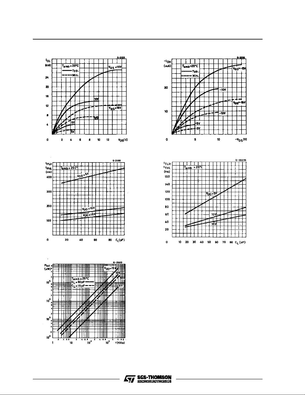
OutputLow (sink)CurrentCharacteristics. OutputHigh (source) Current Characteristics.
TypicalPropagation Delay Time vs.Load Capacitance
TypicalDynamicPower Dissipation vs. Input Frequen
(for A or B to F, logic mode).
7/12
Page 8

HCC/HCF40181B
TEST CIRCUITS
QuiescentDevice Current. Input Voltage.
Input Leakage Current. DynamicPower Dissipation.
8/12
Page 9
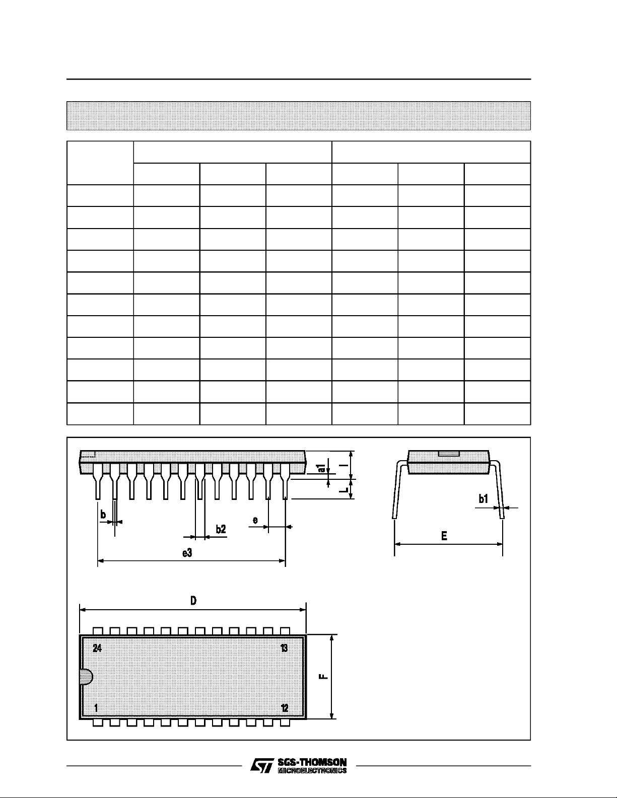
Plastic DIP24 (0.25) MECHANICAL DATA
HCC/HCF40181B
DIM.
MIN. TYP. MAX. MIN. TYP. MAX.
a1 0.63 0.025
b 0.45 0.018
b1 0.23 0.31 0.009 0.012
b2 1.27 0.050
D 32.2 1.268
E 15.2 16.68 0.598 0.657
e 2.54 0.100
e3 27.94 1.100
F 14.1 0.555
I 4.445 0.175
L 3.3 0.130
mm inch
P043A
9/12
Page 10

HCC/HCF40181B
Ceramic DIP24 MECHANICAL DATA
DIM.
MIN. TYP. MAX. MIN. TYP. MAX.
A 32.3 1.272
B 13.05 13.36 0.514 0.526
C 3.9 5.08 0.154 0.200
D 3 0.118
E 0.5 1.78 0.020 0.070
e3 27.94 1.100
F 2.29 2.79 0.090 0.110
G 0.4 0.55 0.016 0.022
I 1.17 1.52 0.046 0.060
L 0.22 0.31 0.009 0.012
M 1.52 2.49 0.060 0.098
N1
P 15.4 15.8 0.606 0.622
Q 5.71 0.225
4° (min.), 15° (max.)
mm inch
10/12
P058C
Page 11
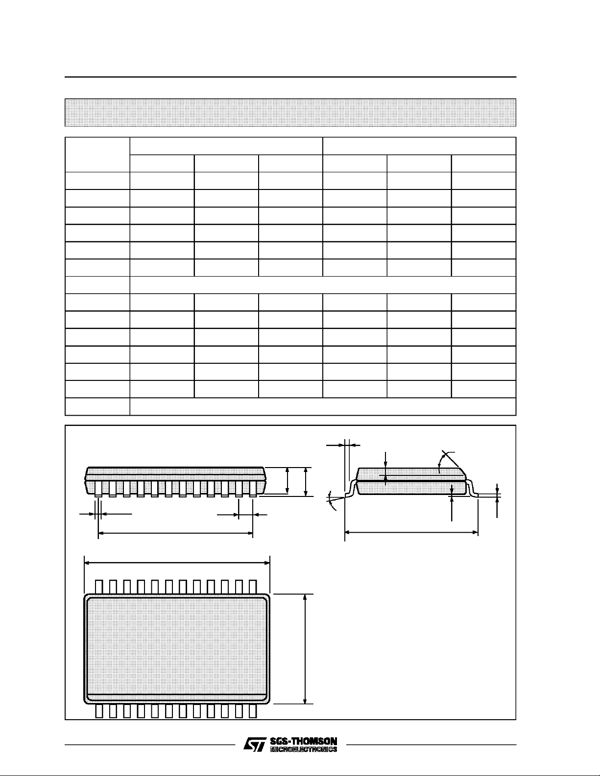
SO24 MECHANICAL DATA
HCC/HCF40181B
DIM.
MIN. TYP. MAX. MIN. TYP. MAX.
A 2.65 0.104
a1 0.10 0.20 0.004 0.007
a2 2.45 0.096
b 0.35 0.49 0.013 0.019
b1 0.23 0.32 0.009 0.012
C 0.50 0.020
c1 45° (typ.)
D 15.20 15.60 0.598 0.614
E 10.00 10.65 0.393 0.420
e 1.27 0.05
e3 13.97 0.55
F 7.40 7.60 0.291 0.299
L 0.50 1.27 0.19 0.050
S8°(max.)
mm inch
L
A
a2
b
e3
D
24 13
112
e
F
s
a1
c1
b1
C
E
11/12
Page 12

HCC/HCF40181B
Information furnished is believed to be accurate and reliable. However, SGS-THOMSON Microelectronics assumes no responsability for the
consequences of use of such information nor for any infringement of patents or other rights of third parties which may results from its use. No
license is granted by implication or otherwise underany patent or patent rights of SGS-THOMSON Microelectronics. Specificationsmentioned
in this publication are subject to changewithout notice. This publication supersedes and replaces all information previously supplied.
SGS-THOMSON Microelectronicsproductsare notauthorized for use ascritical componentsinlife supportdevices or systemswithout express
written approval of SGS-THOMSON Microelectonics.
1994 SGS-THOMSON Microelectronics - All RightsReserved
Australia - Brazil - France - Germany - Hong Kong - Italy - Japan - Korea - Malaysia - Malta - Morocco - The Netherlands -
Singapore - Spain - Sweden - Switzerland - Taiwan - Thailand - United Kingdom - U.S.A
SGS-THOMSON Microelectronics GROUP OF COMPANIES
12/12
 Loading...