

SGS Thomson Microelectronics HCF40174B Datasheet
.STANDARDIZED SYMMETRICAL OUTPUT
CHARACTERISTICS
.QUIESCENT CURRENT SPECIFIED AT 20V
FOR HCC DEVICE
.5V, 10V,AND 15V PARAMETRIC RATINGS
.INPUTCURRENTOF100nA AT18VAND25°C
FOR HCC DEVICE
.100% TESTEDFOR QUIESCENTCURRENT
.MEETSALLREQUIREMENTSOFJEDECTEN-
TATIVE STANDARD No. 13A, ”STANDARD
SPECIFICATIONS FOR DESCRIPTIONOF ”B”
SERIESCMOS DEVICES”
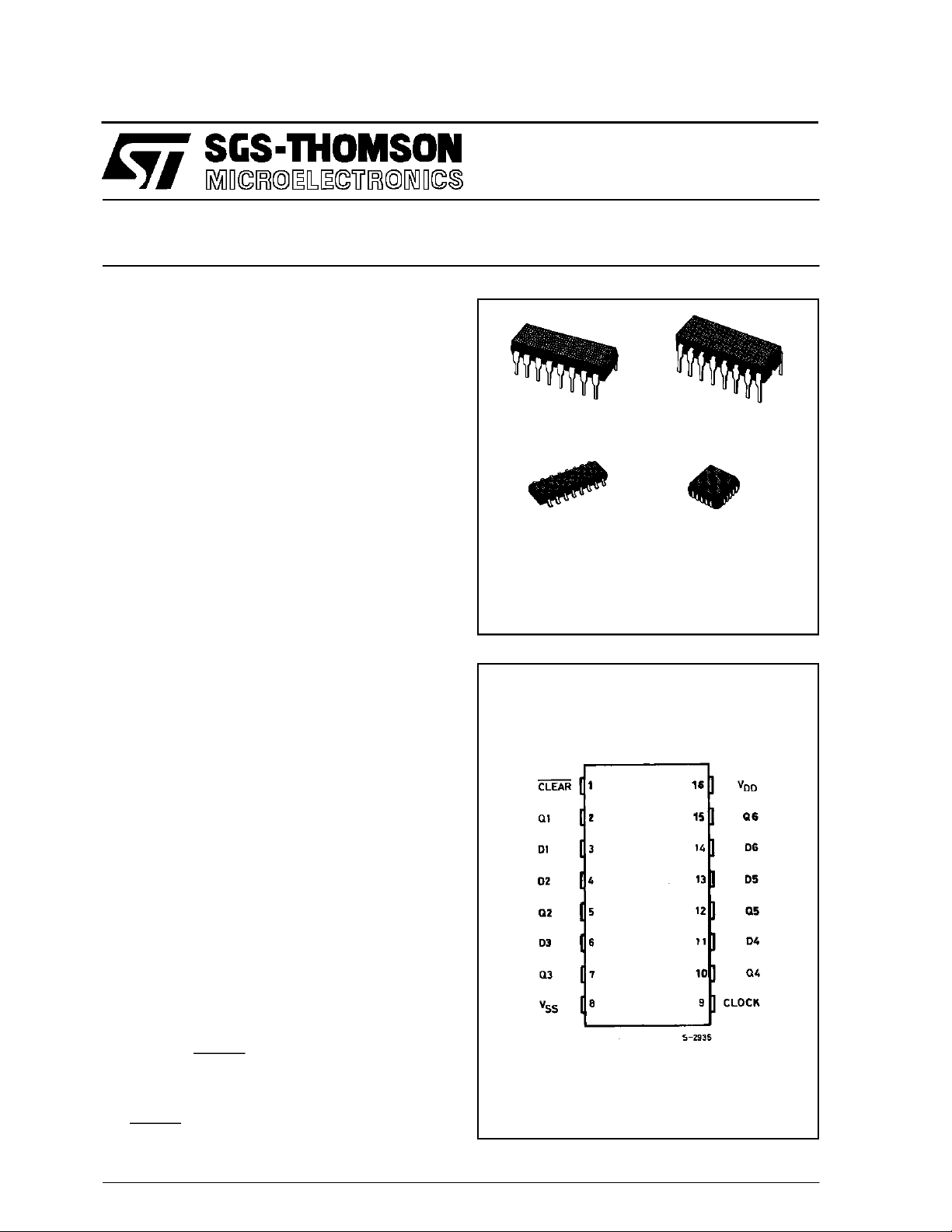
HCC/H CF4 01 74B
HEX ”D” – TYPE FLIP–FLOP
EY
(Plastic Package)
M1
(MicroPackage)
ORDERCODES :
HCC40174BF HCF40174BM1
HCF40174BEY HCF40174BC1
(Ceramic Frit SealPackage)
(Plastic Chip Carrier)
F
C1
DESCRIPTION
The HCC40174B (extended temperature range)
andHCF40174B (intermediate temperature range)
are monolithic integrated circuits available in 16lead dual in-line plastic or ceramic package and
plasticmicropackage.
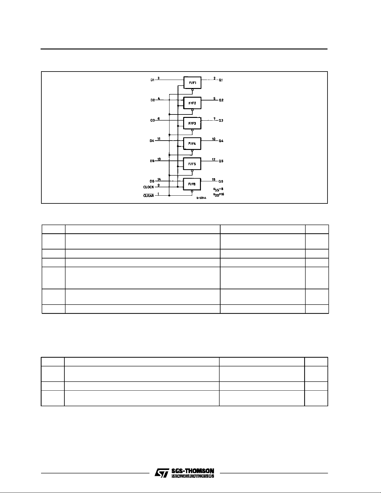
The HCC/HCF40174B consistsof six identical ’D’ -
typeflip-flopshavingindependent DATAinputs.The
CLOCK and CLEAR inputs are common to all six
units. Data is transferred to the Q outputs on the
positive-going transition of the clock pulse. All six
flip-flopsare simultaneously reset by a low levelon
the CLEAR input.
PIN CONNECTIONS
June 1989
1/12
HCC/HCF40174B
FUNCTIONAL DIAGRAM
ABSOLUTE MA XIM UM RATIN GS
Symbol Parameter Value Unit
V
* Supply Voltage : HCC Types
DD
HCF Types
V
Input Voltage – 0.5 to VDD+ 0.5 V
i
I
DC Input Current (any one input) ± 10 mA
I
P
Total Power Dissipation (per package)
tot
– 0.5 to + 20
– 0.5 to + 18
200
V
V
mW
Dissipation per Output Transistor
for Top= Full Package-temperature Range
T
Operating Temperature : HC C Types
op
HCF Types
T
Stresses above those listed under ”Absolute Maximum Ratings” may cause permanent damage to the device. This is a stress
rating only and functional operation of the device at these or any other conditions above those indicated in the operational sections of this specification is not implied. Exposure to absolute maximum rating conditions for external periods may affect device
reliability.
Storage Temperature – 65 to + 150 °C
stg
100
–55to+125
–40to+85
mW
°C
°C
RECOMMENDED OPERATING CONDITIONS
Symbol Parameter Valu e Unit
V
Supply Voltage : HCC Types
DD
HCF Types
V
Input Voltage 0 to V
I
T
Operating Tem perature : HCC Types
op
HCF Types
3to18
3to15
DD
– 55 to + 125
–40to+85
V
V
V
°C
°C
2/12
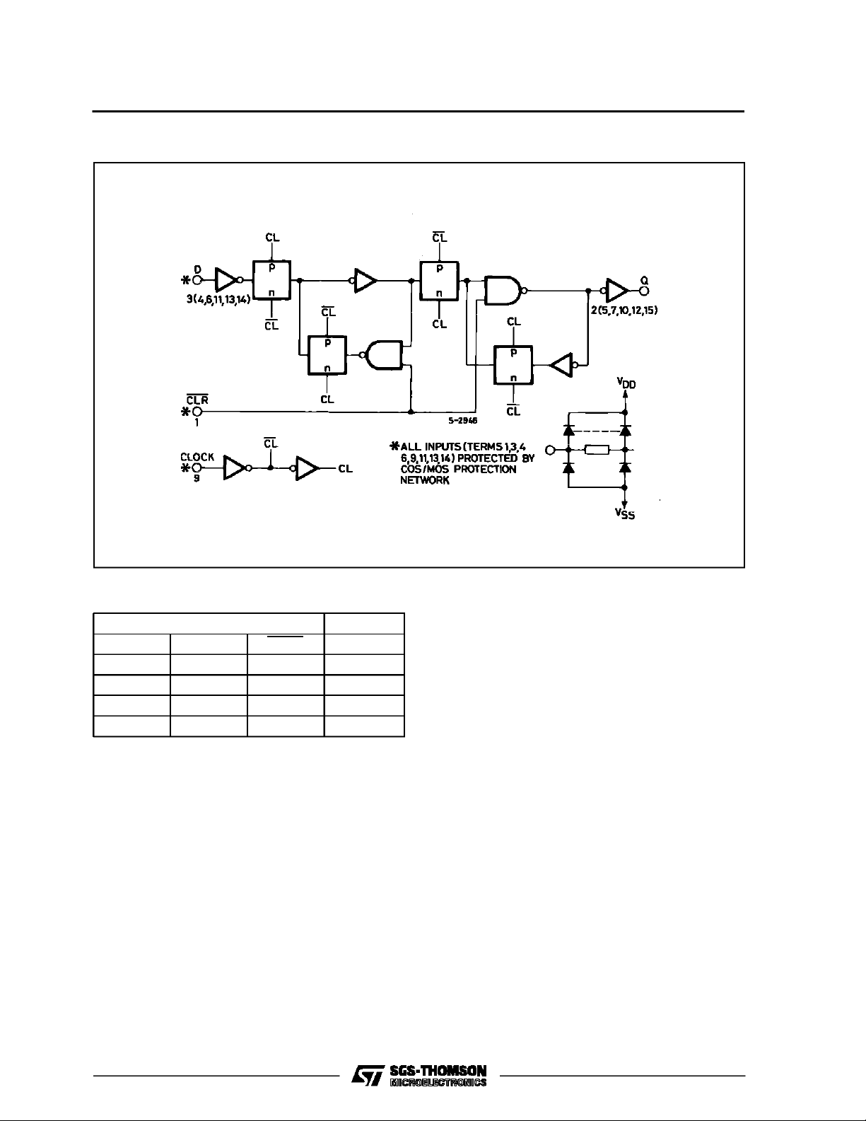
LOGIC DIAGRAM (1 of 6 Flip-Flops)
HCC/HCF40174B
TRUTH TABLE
Inputs Output
ClockDataClear Q
–
/
–
–
/
–
–
\
–
XX0 0
1 = High Level X = Don’t Care
0 = Low Level NC = No Change
010
111
X1NC
3/12
HCC/HCF40174B
STATIC ELECTRICAL CHARACTERISTICS (over recommended operating conditions)
Test Conditions Valu e
Symbol Parameter
I
Quiescent
L
Current
HCC
Types
HCF
Types
V
OH
Output High
Voltage
V
OL
Output Low
Voltage
V
IH
Input High
Voltage
V
IL
Input Low
Voltage
I
OH
Output
Drive
Current
HCC
Types
HCF
Types
I
OL
Output
Sink
Current
HCC
Types
HCF
Types
I
IH,IIL
Input
Leakage
Current
HCC
Types
HCF
Types
Input Capacitance Any Input 5 7.5 pF
C
I
*T
=–55°CforHCC device : – 40°C for HCF device.
Low
*T
= + 125°C for HCC device : + 85°C for HCF device.
High
TheNoiseMargin for both ”1” and ”0” levelis : 1V min.with VDD=5V, 2V min.withVDD= 10V,2.5 V min.with VDD= 15V.
V
V
O
|IO|V
I
(V) (V) (µA) (V)
T
DD
* 25°CT
Low
Min. Max. Min. Typ. Max. Min. Max.
High
0/ 5 5 1 0.02 1 30
0/10 10 2 0.02 2 60
0/15 15 4 0.02 4 120
0/20 20 20 0.04 20 600
0/ 5 5 4 0.02 4 30
0/10 10 8 0.02 8 60
0/15 15 16 0.02 16 120
0/ 5 < 1 5 4.95 4.95 4.95
0/10 < 1 10 9.95 9.95 9.95
0/15 < 1 15 14.95 14.95 14.95
5/0 < 1 5 0.05 0.05 0.05
10/0 < 1 10 0.05 0.05 0.05
15/0 < 1 15 0.05 0.05 0.05
0.5/4.5 < 1 5 3.5 3.5 3.5
1/9 < 1 10 7 7 7
1.5/13.5 < 1 15 11 11 11
4.5/0.5 < 1 5 1.5 1.5 1.5
9/1 < 1 10 3 3 3
13.5/1.5 < 1 15 4 4 4
0/ 5 2.5 5 – 2 – 1.6 – 3.2 – 1.15
0/ 5 4.6 5 – 0.64 – 0.51 – 1 – 0.36
0/10 9.5 10 – 1.6 – 1.3 – 2.6 – 0.9
0/15 13.5 15 – 4.2 – 3.4 – 6.8 – 2.4
0/ 5 2.5 5 – 1.53 – 1.36 – 3.2 – 1.1
0/ 5 4.6 5 – 0.52 – 0.44 – 1 – 0.36
0/10 9.5 10 – 1.3 – 1.1 – 2.6 – 0.9
0/15 13.5 15 – 3.6 – 3.0 – 6.8 – 2.4
0/ 5 0.4 5 0.64 0.51 1 0.36
0/10 0.5 10 1.6 1.3 2.6 0.9
0/15 1.5 15 4.2 3.4 6.8 2.4
0/ 5 0.4 5 0.52 0.44 1 0.36
0/10 0.5 10 1.3 1.1 2.6 0.9
0/15 1.5 15 3.6 3.0 6.8 2.4
0/18
18 ± 0.1 ±10
–5
± 0.1 ± 1
Any Input
0/15
15 ± 0.3 ±10
–5
± 0.3 ± 1
Unit
*
µA
V
V
V
V
mA
mA
µA
4/12
 Loading...