


HCC/HCF4016B
QUAD BILATERAL SWITCH
.20V DIGITAL OR ± 10 V PEAK-TO-PEAK
SWITCHING
.280Ω TYPICAL ON RESISTANCE FOR 15V
OPERATION
.SWITCH ON RESISTANCE MATCHED TO
WITHIN 10Ω TYP. OVER 15V SIGNAL INPUT
RANGE
.HIGH ON/OFF OUTPUT-VOLTAGE RATIO :
65dB TYP.@ fis=10kHz, RL= 10kΩ
.HIGH DEGREE OF LINEARITY : < 0.5% DIS-
TORTIONTYP. @ fis= 1KHz, Vis=5Vpp,VDDVSS≥ 10V, RL=10kΩ
.EXTREMELY LOW OFF SWITCH LEAKAGE
RESULTING IN VERY LOW OFFSET CURRENT AND HIGH EFFECTIVE OFF RESISTANCE: 100pA TYP. @ VDD-VSS= 18V, T
25°C
amb
.EXTREMELY HIGHCONTROL INPUT IMPED-
ANCE (control circuitisolated from signalcircuit
1012Ω typ.)
.LOW CROSSTALK BETWEEN SWITCHES :
50dB TYP.@ fis= 0.9MHz, RL=1kΩ
.MATCHED CONTROL-INPUT TO SIGNAL-
OUTPUT CAPACITANCE : REDUCES OUTPUT SIGNAL TRANSIENTS
.FREQUENCY RESPONSE’ SWITCH ON =
40MHz (typ.)
.QUIESCENT CURRENT SPECIFIED TO 20V
FOR HCC DEVICE
.5V, 10V,AND 15VPARAMETRIC RATINGS
.INPUT CURRENTOF100nA AT18VAND25°C
FOR HCC DEVICE
.100% TESTEDFOR QUIESCENTCURRENT
.MEETSALLREQUIREMENTSOFJEDECTEN-
TATIVESTANDARDN°13A,”STANDARD SPECIFICATIONS FOR DESCRIPTION OF ”B”
SERIESCMOS DEVICES”
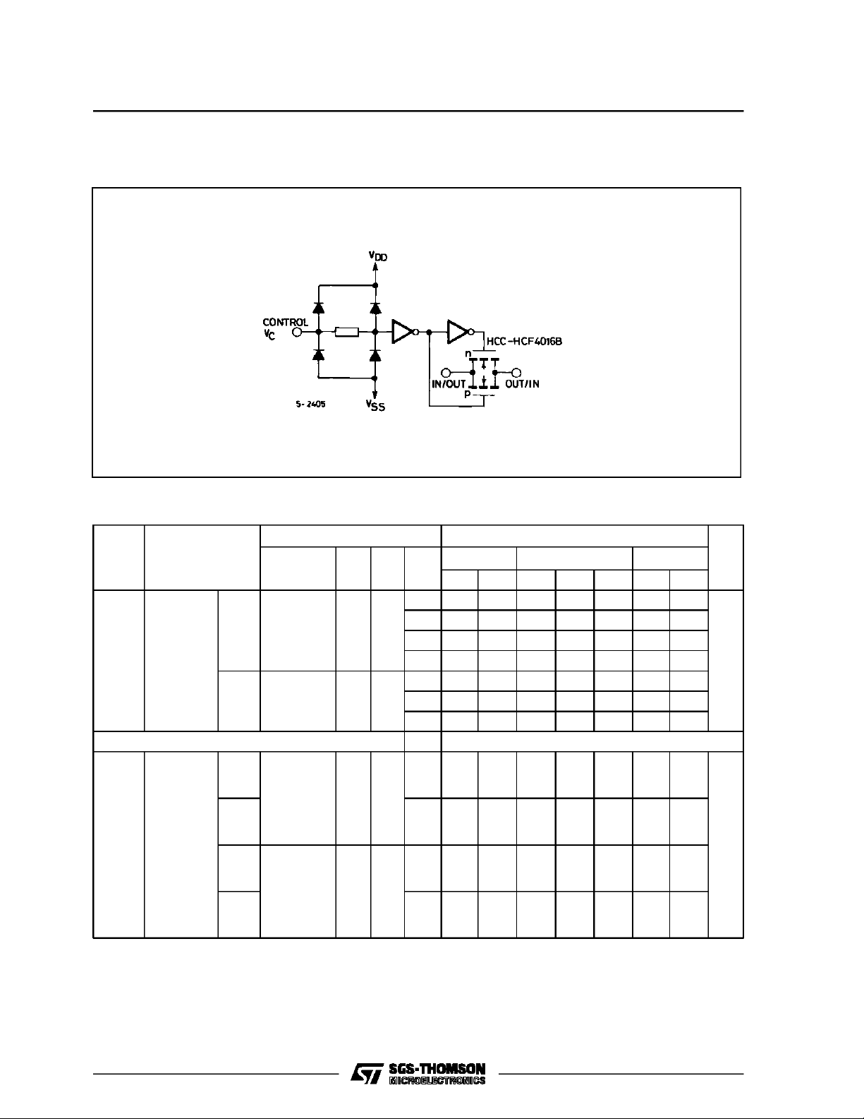
of analog or digital signals. Each of the four independent bilateral switches has a single control signal
input which simultaneously biases both the p and n
device in a given switchONorOFF.
EY
(Plastic Package)F(Ceramic Frit Seal Package)
=
M1
(MicroPackage)
ORDER CODES :
HCC4016BF HCF4016BM1
HCF4016BEY HCF4016BC1
PIN CON NEC TI O NS
(Plastic Chip Carrier)
C1
DESCRIPTION
TheHCC4016B(extended temperature range) and
HCF4016B (intermediate temperature range) are
monolithic integrated circuit, available in 14-lead
dual in-line plastic or ceramic package and plastic
micropackage.
TheHCC/HCF4016B Series types are quad bilateral
switchesintendedforthetransmission ormultiplexing
June1989
1/15

HCC/HCF4016B
FUNCTIONAL DIAGRAM
ABSOLUTE M AXI MUM RAT I N GS
Symbol Parameter Value Unit
V
* Supply Voltage : HCC Types
DD
HCF Types
V
Input Voltage – 0.5 to VDD+ 0.5 V
i
I
DC Input Current (any one input) ± 10 mA
I
P
Total Power Dissipation (per package)
tot
Dissipation per Output Transistor
for T
T
Operating Temperature : HCC Types
op
= Full Package-temperature Range
op
HCF Types
T
Stresses above those listed under ”Absolute Maximum Ratings” may cause permanent damage to the device. This is a stress
rating only and functional operation of the device at these or any other conditions above those indicated in the operational sections of this specification is not implied. Exposure to absolute maximum rating conditions for external periods may affect device
reliability.
* All voltage values are referred to VSSpin voltage.
Storage Temperature – 65 to + 150 °C
stg
– 0.5 to + 20
– 0.5 to + 18
200
100
– 55 t o + 125
–40to+85
V
V
mW
mW
°C
°C
RECOMMENDED OPERATING CONDITIONS
Symbol Parameter Value Unit
V
T
2/15
Supply Voltage : HCC Types
DD
HCF Types
V
Input Voltage 0 to V
I
Operating Temperature : HCC Types
op
HCF Types
3to18
3to15
DD
– 55 t o + 125
–40to+85
V
V
V
°C
°C
HCC/HCF4016B
SCHEMATIC DIAGRAM
1 OF 4 IDENTICAL SECTION
STATIC ELECTRICAL CHARACTERISTICS (over recommended operating conditions)
Test Conditions Value
V
Symbol Parameter
I
Quiescent
L
Device
Current (all
HCC
Types
C=VSSVDD
V
(V) (V)
DD
switches
on or all
switches
off)
HCF
Types
SWITCH V
R
ON
Resistance
HCC
R
=10kΩ• + 7.5 – 7.5
L
HCF
HCC
R
=10kΩ• +5 –5
L
HCF
*T
=–55°CforHCC device : – 40°CforHCF device.
Low
*T
=+125°C for HCC device : + 85°C for HCF device.
High
T
* 25°CT
Low
High
Min. Max. Min. Typ. Max. Min. Max.
5 0.25 0.01 0.25 7.5
10 0.5 0.01 0.5 15
15 1 0.01 1 30
20 5 0.02 5 150
5 1 0.01 1 7.5
10 2 0.01 2 15
15 4 0.01 4 30
IS
+ 7.5
– 7.5
± 0.25
+ 7.5
– 7.5
± 0.25
+5
–5
±0.25
+5
–5
±0.25
360
360
775
370
370
790
600
600
1870
610
610
1900
200
200
280
200
200
280
250
250
580
250
250
580
400
400
850
400
400
850
660
660
2000
660
660
2000
*
600
600
1230
520
520
1080
960
960
2600
840
840
2380
Unit
µA
Ω
3/15

HCC/HCF4016B
STATIC ELECTRICAL CHARACTERISTICS (continued)
Test Conditions Value
V
Symbol Parameter
SWITCH (continued)
ON
Resistance
R
HCC
=10kΩ•
R
L
HCF
HCC
R
=10kΩ•
L
HCF
∆ON Resistance ∆RON
(between any 2
of 4 switches)
R
L
=10kΩ•
Input or Output
Leakage Current
HCC
Switch OFF
(effective off
resistance)
C
I
C
O
Input Capacitance
Output
HCF
V
CC=VSS
Capacitance
C
CONTRO L (V
V
Feedthrough
IO
Switch Threshold
TH
Voltage I
I
Input
I
Current
)
C
=10µA
IS
HCC
Types
≤ V
V
IS
HCF
Types
C
Input Capacitance 5
I
*T
=–55°CforHCC device : – 40°CforHCF device.
Low
*T
=+125°C for HCC device : + 85°C for HCF device.
High
C=VSSVDD
(V) (V)
V
DD
Min. Max. Min. Typ. Max. Min. Max.
+15
+15 0
+ 0.25
+ 9.3
+15
+15 0
+ 0.25
+ 9.3
+10
+10 0
+ 0.25
+ 5.6
+10
+10 0
+ 0.25
+ 5.6
+ 7.5 – 7.5 ± 7.5 10
+5 –5 ±515
V
V
DD
+18
V
DD
+15
=
C
V
SS
0 ±0.1 10–5± 0.1 1
V
=
C
V
SS
0 ±0.3 10–5± 0.3 1
=–5 +5
5 1 1 2.25 1
10 2 2 4.5 2
15 2 2 6.75 2
18 ± 0.1 ±10–5± 0.1 ± 1
DD
15 ± 0.3 ±10
T
* 25°CT
Low
360
360
775
370
370
790
600
600
1870
610
610
1900
200
200
300
200
200
300
250
250
560
250
250
560
400
400
850
400
400
800
660
660
2000
660
660
2000
4
4
0.2
–5
± 0.3 ± 1
7.5 pF
High
*
600
600
1230
520
520
1080
960
960
2600
840
840
2380
Unit
Ω
Ω
µA
pF
V
µA
4/15

HCC/HCF4016B
DYNAMIC ELECTRICAL CHARACTERISTICS (T
wave rise and fall time = 20ns)
Test Conditions Value
Parameter
(V)
V
C
SWITCH
Propagation Delay Time
t
pd
(signal intput to output)
=V
DD
Crosstalk Between any 2 of 4
Switches (f @ – 50dB)
V
O(B)
20 log 10 = – 50dB
____
V
I(A)
V
C(A)=VDD
V
C(B)=VSS
Frequency Response Switch
”ON” (sine wave input)
At 20 log 10 = – 3dB
Feedtrough (switch OFF)
At 20 log 10 = – 50dB
V
O
____
V
I
V
O
____
V
I
Sine Wave Distortion = V
=V
DD
=+5
=V
SS
=–5
DD
=5
CONTROL (V
)
C
Propagation Delay :
V
(turn on control to
output)
Max. Allowable Control Input
Repetition Rate
Crosstalk (control input to
signal output)
(∆) Symmetrical about OV (•) Forall testconditions.
DD–VSS
(sq. wawe)
10 (sq. wawe) 1 V
10 (sq. wave) 10 GND 10 50 mV
R
L
(kΩ)
(KHz)
10
=+5
=–5
1
1 5p-p – 5 40 MHz
1 – 5p-p 5 1.25 MHz
10 1 5p-p – 5 0.4 %
1
=25°C, CL= 50pF all input square
amb
f
V
V
i
I
(V)
(V)
ss
V
DD
(V)
540100
10sq.
GND
Wave
10 20 50
15 15 40
V
I(A)
∆
= 5p-p
V
DD
or
V
SS
GND 10 10 MHz
DD
5
V
10 20 40
DD–VSS
15 15 30
= 10V
Typ. Max.
Unit
0.9 MHz
35 70
ns
ns
Typical ”ON”Characteristics for 1 of 4 switches with VDD= + 15V, VSS=0V, and Test Circuit.
5/15

HCC/HCF4016B
Typical ”ON”Characteristics for 1 of 4 switcheswithVDD=+ 10V, VSS= 0V, andTest Circuit.
Typical ”ON”Characteristics for 1 of 4 switches with VDD= + 5V, VSS=0V, and Test Circuit.
Typical ”ON”Characteristics for 1 of 4 switches with VDD= + 7.5V, VSS= – 7.5V, andTest Circuit.
6/15

HCC/HCF4016B
Typical ”ON”Characteristics for 1 of 4 switcheswithVDD=+ 5V, VSS= – 5V, and Test Circuit.
Typical ”ON”Characteristics for 1 of 4 switches with VDD= + 2.5V, VSS= – 2.5V, andTest Circuit.
Typical ”ON”Characteristics as function of temp.for1 of 4 switcheswith VDD=+ 5V and Test Circuit.
7/15

HCC/HCF4016B
Typical feedthruvs. frequency-switch”OFF” and Test Circuit.
Typical Crosstalkbetween Switch Circuits in the Same Package.
TypicalSwitch Frequency response-switch ” ON” andTest Circuit.
8/15

HCC/HCF4016B
TYPICAL ”ON” RESISTANCE CHARACTERISTICS, T
Supply
Characte ri st i c*
R
ON
(max) + 15 0 300 + 11 300 + 9.3 320 + 9.2
R
ON
R
ON
R
(max) + 10 0 500 + 7.4 560 + 5.6 610 +5.5
ON
R
ON
(max) + 5 0 1.7k + 4.2 7k + 2.9 33k +2.7
R
ON
R
ON
(max) + 2.5 – 2.5 232k ± 0.25 300k ± 0.25 870k ± 0.25
R
ON
* Variation from a perfect switch, RON=0Ω.
Conditions
V
DD
(V)
V
SS
(V)
+15 0
+10 0
+5 0
+ 2.5 – 2.5
R
=1kΩ RL=10kΩ RL= 100 kΩ
L
Valu e
(Ω)
V
(V)
is
200 + 15 200 + 15 180 + 15
200020002000
290 + 10 250 + 10 240 + 10
290025003000
860+5470+5450+5
600058008000
590 + 2.5 450 + 2.5 490 + 2.5
720 – 2.5 520 – 2.5 520 – 2.5
=25°C
amb
Load Conditions
Value
(Ω)
V
(V)
is
Value
(Ω)
TEST CIRCUITS
”OFF” SwitchInputor Put Leakage Current.
Square-Wave Response.
V
(V)
is
9/15

HCC/HCF4016B
TEST CIRCUITS (continued)
Crosstalk-control Input to Signal Output. Propagaton DelayTime Signal Input (VIS) to Sig-
nal Output (VOS).
Max Allowable Control-input Repetition Rate. Switch Treshold Voltage.
Capacitance C
10/15
andCOS.
IOS
Turn-OnPropagation Delay-control Inputto Output.

Plastic DIP14 MECHANICAL DATA
HCC/HCF4016B
DIM.
MIN. TYP. MAX. MIN. TYP. MAX.
a1 0.51 0.020
B 1.39 1.65 0.055 0.065
b 0.5 0.020
b1 0.25 0.010
D 20 0.787
E 8.5 0.335
e 2.54 0.100
e3 15.24 0.600
F 7.1 0.280
I 5.1 0.201
L 3.3 0.130
Z 1.27 2.54 0.050 0.100
mm inch
P001A
11/15

HCC/HCF4016B
Ceramic DIP14/1 MECHANICAL DATA
DIM.
MIN. TYP. MAX. MIN. TYP. MAX.
A 20 0.787
B 7.0 0.276
D 3.3 0.130
E 0.38 0.015
e3 15.24 0.600
F 2.29 2.79 0.090 0.110
G 0.4 0.55 0.016 0.022
H 1.17 1.52 0.046 0.060
L 0.22 0.31 0.009 0.012
M 1.52 2.54 0.060 0.100
N 10.3 0.406
P 7.8 8.05 0.307 0.317
Q 5.08 0.200
mm inch
12/15
P053C

SO14 MECHANICAL DATA
HCC/HCF4016B
DIM.
MIN. TYP. MAX. MIN. TYP. MAX.
A 1.75 0.068
a1 0.1 0.2 0.003 0.007
a2 1.65 0.064
b 0.35 0.46 0.013 0.018
b1 0.19 0.25 0.007 0.010
C 0.5 0.019
c1 45° (typ.)
D 8.55 8.75 0.336 0.344
E 5.8 6.2 0.228 0.244
e 1.27 0.050
e3 7.62 0.300
F 3.8 4.0 0.149 0.157
G 4.6 5.3 0.181 0.208
L 0.5 1.27 0.019 0.050
M 0.68 0.026
S8°(max.)
mm inch
P013G
13/15

HCC/HCF4016B
PLCC20 MECHANICAL DATA
DIM.
MIN. TYP. MAX. MIN. TYP. MAX.
A 9.78 10.03 0.385 0.395
B 8.89 9.04 0.350 0.356
D 4.2 4.57 0.165 0.180
d1 2.54 0.100
d2 0.56 0.022
E 7.37 8.38 0.290 0.330
e 1.27 0.050
e3 5.08 0.200
F 0.38 0.015
G 0.101 0.004
M 1.27 0.050
M1 1.14 0.045
mm inch
14/15
P027A

HCC/HCF4016B
Information furnished is believed tobe accurate and reliable. However, SGS-THOMSON Microelectronics assumes no responsability for the
consequences of use of such information nor for any infringementofpatents orother rights of third parties which may results from its use. No
license isgrantedby implication or otherwiseunder any patent orpatentrights of SGS-THOMSONMicroelectronics.Specificationsmentioned
in this publication are subject to changewithout notice.This publication supersedes andreplaces all information previously supplied.
SGS-THOMSON Microelectronicsproductsare notauthorizedforuse ascritical componentsin life supportdevices orsystemswithout express
written approval of SGS-THOMSON Microelectonics.
1994 SGS-THOMSON Microelectronics - All RightsReserved
Australia - Brazil - France - Germany - Hong Kong - Italy - Japan - Korea - Malaysia-Malta - Morocco - The Netherlands -
Singapore - Spain - Sweden - Switzerland - Taiwan - Thailand - UnitedKingdom - U.S.A
SGS-THOMSON MicroelectronicsGROUPOF COMPANIES
15/15
 Loading...