

Datasheet HCF40163B, HCF40162B, HCF40161B, HCF40160B Datasheet (SGS Thomson Microelectronics)
Page 1
SYNCHRONOUS PROGRAMMABLE 4-BIT COUNTERS
40160B - DECADE WITH ASYNCHRONOUS
CLEAR
40161B - BINARY WITH ASYNCHRONOUS
CLEAR
40162B - DECADE WITH SYNCHRONOUS
CLEAR
40163B - BINARY WITH SYNCHRONOUS
CLEAR
.INTERNAL LOOK-AHEADFOR FAST COUNT-
ING
.CARRY OUTPUT FOR CASCADING
.SYNCHRONOUSLY PROGRAMMABLE
.LOW-POWER TTL COMPATIBILITY
.STANDARDIZED SYMMETRICAL OUTPUT
CHARACTERISTICS
.QUIESCENT CURRENT SPECIFIED AT 20V
FOR HCC DEVICE
.5V, 10V AND 15V PARAMETRIC RATINGS
.INPUT CURRENTOF100nAAT18VAND 25oC
FOR HCC DEVICE
.100% TESTEDFOR QUIESCENTCURRENT
.MEETSALLREQUIREMENTSOFJEDECTEN-
TATIVE STANDARD N. 13A, ” STANDARD
SPECIFICATIONS FOR DESCRIPTION OF B
SERIESCMOS DEVICES ”
HCC/HCF40160B-40161B
HCC/HCF40162B-40163B
EY
(PlasticPackage)
M1
(MicroPackage)
ORDER CODES :
HCC40XXXBF HCF40XXX BEY
(CeramicPackage)
HCF40XXX BC1
F
C1
(Chip Carrier)
DESCRIPTION
The HCC40160B, 40161B, 40162B, 40163B (ex-
tended temperature range) and HCF40160B,
40161B, 40162B, 40163B (intermediate temperature range) are monolithic integrated circuits,available in 16-lead dual in line plastic or ceramic
package and plastic micropackage.
HCC/HCF40160B, 40161B, 40162B and 40163B
are4-bitsynchronous programmable counters. The
CLEAR function of the HCC/HCF40162B and
40163Bissynchronousand a low ontheat the clear
CLEAR input sets all four outputs low on the next
positiveCLOCK edge. The CLEAR function of the
HCC/HCF40160B and 40161B is asynchronous
and alowlevel at the CLEAR inputsets allfour outputs low regardless of the state of the CLOCK,
LOAD or ENABLEinputs. A low level at theLOAD
inputdisables thecounter and causes the output to
agree with the set-up data after the next CLOCK
pulseregardless oftheconditions oftheENABLE in-
September 1988
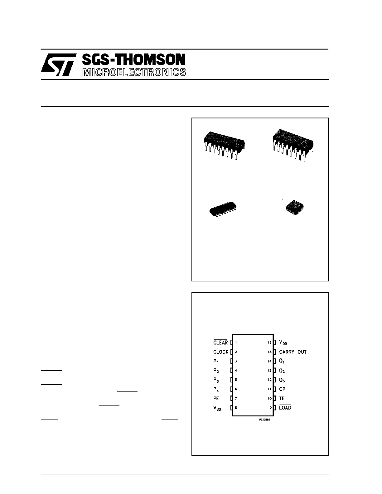
PIN CONNECTIONS
1/15
Page 2
HCC/H CF40160B-40161B-40162-40163
cascadingcounter for n-bit synchronour application
without additional gating. Instrumental in accomplishing this function are two count-enable input
and a carry output (COUT). Counting is enable
when bothPE and TEinputs arehigh. The TEinput
is fed forward to enable COUT. This enableoutput
produces apositive outputpulsewith a durationapproximately equal to the positiveportion of the Q1
output. This positive overflow carry pulse can be
used to enable successive cascadedstages. Logic
transitionsat the PE or TE inputs may occurwhen
the clock is eitherhigh orlow.
ABSOLU TE MAXIMUM RATI NG
Symbol Parameter Value Unit
* Supply Voltage: HCC Types
V
DD
HCF Types
V
P
Input Voltage -0.5 to VDD+ 0.5 V
i
I
DC Input Current (any one input) ± 10 mA
I
Total Power Dissipation (per package)
tot
Dissipation per Output Transistor
for Top = Full Package Temperature Range
T
Operating Temperature: HCC Types
op
HCF Types
T
Stressesabove thoselistedunder ”Absolute Maximum Ratings”maycause permanent damage tothedevice. Thisisa stressratingonly and functional
operationofthedevice atthese or anyother conditions above thoseindicated intheoperational sections of thisspecification is not implied.Exposure
to absolute maximum rating conditions forexternal periods may affect device reliability.
* All voltagevalues are referred to VSSpinvoltage.
Storage Temperature -65 to +150
stg
-0.5 to +20
-0.5 to +18
200
100
-55 to +125
-40 to +85
V
V
mW
mW
o
C
o
C
o
C
RECO MM ENDED OPERATIN G C O NDITI ONS
Symbol Parameter Value Unit
V
Supply Voltage: HCC Types
DD
HCF Types
V
T
Input Voltage 0 to V
I
Operating Temperature: HCC Types
op
HCF Types
3to18
3to15
DD
-55 to +125
-40 to +85
TRUTH TABLE
Clock CLR LOAD PE TE Operation
1 0 X X Preset
110XNC
11X0NC
1 1 1 1 Count
X 0 X X X Reset (HCC/HCF40160B, HCC/HCF40161B)
0 X X X Reset (HCC/HCF40162B, HCC/HCF40163B)
1 X X X NC (HCC/HCF40162B, HCC/HCF40163B)
1 = HIGHLEVEL,0 = LOW LEVEL,X= DON’T CARE,NC = NOCHANGE
V
V
V
o
C
o
C
2/15
Page 3
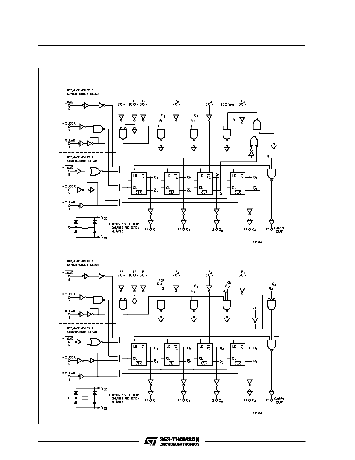
LOGI C DIAG RAM S
HCC/ HCF40160B-40161B-40162B-40163B
HCC4 0160B/HC C40162B
HCC4 0161B/HC C40163B
3/15
Page 4
HCC/H CF40160B-40161B-40162-40163
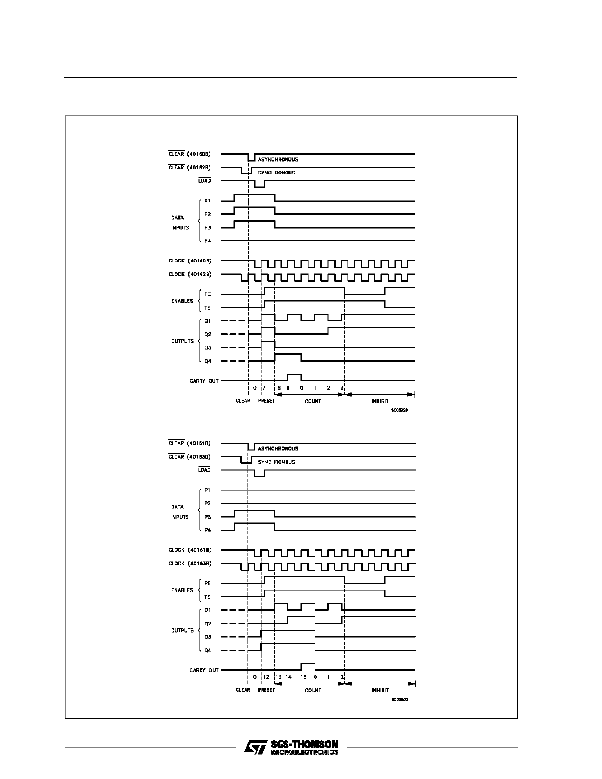
TIM ING DIAGR AMS
HCC4 0160B/HC C40162B
HCC4 0161B/HC C40163B
4/15
Page 5
HCC/ HCF40160B-40161B-40162B-40163B
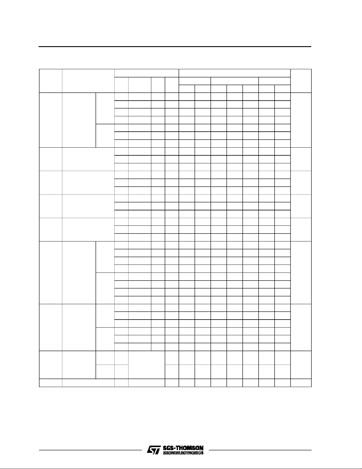
STATI C ELECTRIC AL CHARACTE R IS TICS (over recommended op erating c onditio ns)
Test Conditios Value
Symbol Parameter
Quiescent
I
L
Current
HCC
Types
V
(V)
V
I
(V)
|IO|
(µA)
V
(V)
O
T
DD
*25
LOW
Min. Max. Min. Typ. Max. Min. Max.
0/5 5 5 0.04 5 150
0/10 10 10 0.04 10 300
0/15 15 20 0.04 20 600
o
CT
0/20 20 100 0.08 100 3000
HCF
Types
0/5 5 20 0.04 20 150
0/10 10 40 0.04 40 300
0/15 15 80 0.04 80 600
OH
Output High
V
Voltage
0/5 < 1 5 4.95 4.95 4.95
0/10 < 1 10 9.95 9.95 9.95
0/15 < 1 15 14.95 14.95 14.95
OL
Output Low
V
Voltage
5/0 < 1 5 0.05 0.05 0.05
10/0 < 1 10 0.05 0.05 0.05
15/0 < 1 15 0.05 0.05 0.05
IH
Input High
V
Voltage
0.5/4.5 < 1 5 3.5 3.5 3.5
1/9 < 1 10 7 7 7
1.5/13.5 < 1 15 11 11 11
IL
Input Low
V
Voltage
4.5/0.5 < 1 5 1.5 1.5 1.5
9/1 < 1 10 3 3 3
13.5/1.5 < 1 15 4 4 4
OH
Output
Drive
Current
HCC
Types
I
0/5 2.5 5 -2 -1.6 -3.2 -1.15
0/5 4.6 5 -0.64 -0.51 -1 -0.36
0/10 9.5 10 -1.6 -1.3 -2.6 -0.9
0/15 13.5 15 -4.2 -3.4 -6.8 -2.4
0/5 2.5 5 -1.53 -1.36 -3.2 -1.1
HCF
Types
0/5 4.6 5 -0.52 -0.44 -1 -0.36
0/10 9.5 10 -1.3 -1.1 -2.6 -0.9
0/15 13.5 15 -3.6 -3.0 -6.8 -2.4
I
OL
Output
Sink
Current
HCC
Types
HCF
Types
0/5 0.4 5 0.64 0.51 1 0.36
0/10 0.5 10 1.6 1.3 2.6 0.9
0/15 1.5 15 4.2 3.4 6.8 2.4
0/5 0.4 5 0.53 0.44 1 0.36
0/10 0.5 10 1.3 1.1 2.6 0.9
0/15 1.5 15 3.6 3.0 6.8 2.4
I
IH,IIL
Input
Leakage
Current
C
*T
LOW
*T
HIGH
TheNoiseMargin for both”1” and”0” levelis: 1Vmin.withVDD=5V, 2 V min.with VDD=10 V,2.5 V min. withVDD=15V
Input Capacitance Any Input 5 7.5 pF
I
=-55oCforHCC device: -40oC for HCF device.
=+125oCforHCC device: +85oC for HCF device.
HCC
Types
HCC
Types
0/18
18 ±0.1 ±10
Any Input
0/15 15 ±0.3 ±10
-5
±0.1 ±1
-5
±0.3 ±1
HIGH
Unit
*
µA
V
V
V
V
mA
mA
µA
5/15
Page 6

HCC/H CF40160B-40161B-40162-40163
DYNAMIC ELECTRICAL CHARACTERISTICS (T
=25oC, CL=50pF,RL= 200 KΩ,
amb
typic al temperat ure coef f ic ent for all VDDvalues is 03 %/oC, all input rise and fall t i mes = 20 ns)
Symbol Parameter
t
PLH
t
PHL
t
PLH
t
PHL
t
PLH
t
PHL
t
setup
Propagation Delay Time
Clock to Q
Propagation Delay Time
Clock to C
OUT
Propagation Delay Time
TE to C
OUT
Setup Time
Data to Clock
t
setup
Setup Time
Load to Clock
t
setup
Setup Time
PE or TE to Clock
t
t
t
t
t
hold
THL
TLH
t
f
rtf
PHL
Hold Time 5 0
Transition Time 5 100 200
CLock Input Pulse Width 5 170 85
W
Maximum Clock Input Frequency 5 2 3
CL
Clock Input Rise or Fall Time * 200
Propagation Delay Time (40160B, 40161B)
Clear to Q
t
setup
Setup Time (40162B, 40163B)
Clear to Clock
t
hold
Hold Time (40162B, 40163B)
Clear to Clock
t
rem
t
Clear Removal Time (40162B, 40163B) 5 200 100
Clear Input Pulse Width Low Level (40160B,
W
40161B)
* If more than oneunitis cascated in theparallelclocked application, tr shouldbe madeless than or equal to thesum ofthe fixedpropagation delay
at 50 pF and thetransition timeof thecarry output drivingstagefor the estimated capacitance
Test Conditions Value
(V) Min. Typ. Max.
V
DD
5 200 400
10 80 160
15 60 120
5 225 450
10 95 190
15 70 140
5 125 250
10 55 110
15 40 80
5 240 120
10 90 45
15 60 30
5 240 120
10 90 45
15 60 30
5 340 170
10 140 70
15 100 50
10 0
15 0
10 50 100
15 40 80
10 70 35
15 50 25
10 5.5 8.5
15 8 12
5 250 500
10 110 220
15 80 160
5 340 170
10 140 70
15 100 50
50
10 0
15 0
10 100 50
15 70 35
5 170 85
10 70 35
15 50 25
70
15
Unit
ns
ns
ns
ns
ns
ns
ns
ns
ns
MHz
ns
ns
ns
ns
ns
ns
6/15
Page 7

HCC/ HCF40160B-40161B-40162B-40163B
Output Low (sink) Current Characteristics
Typical Propagation Delay Time vs Load Capacitance
Output High (source) Current Characteristics
Typical Transition Time vs Load Capacitance
Typical Dynamic Power Dissipation vs Input Frequency
7/15
Page 8

HCC/H CF40160B-40161B-40162-40163
TYPICAL APPLI CA TI ONS
Detail of Flip-flops For 40160B And 40161B (Asynchronous Clear)
Detail of Flip-flops For 40162B And 40163B (Synchronous Clear)
8/15
Page 9

HCC/ HCF40160B-40161B-40162B-40163B
Cascading Counter Packages In The Parallel-Clocked Mode
Cascading Counter Packages In The Ripple-Clocked Mode
9/15
Page 10

HCC/H CF40160B-40161B-40162-40163
TEST CIRCUIT
QuiescentDevice Current. Input Voltage.
Input Leakage Current. DinamicPowerDissipation
10/15
Page 11

HCC/ HCF40160B-40161B-40162B-40163B
Plastic DIP16 (0.25) MECHANICAL DATA
DIM.
MIN. TYP. MAX. MIN. TYP. MAX.
a1 0.51 0.020
B 0.77 1.65 0.030 0.065
b 0.5 0.020
b1 0.25 0.010
D 20 0.787
E 8.5 0.335
e 2.54 0.100
e3 17.78 0.700
F 7.1 0.280
I 5.1 0.201
L 3.3 0.130
Z 1.27 0.050
mm inch
P001C
11/15
Page 12

HCC/H CF40160B-40161B-40162-40163
Ceramic DIP16/1 MECHANICAL DATA
DIM.
MIN. TYP. MAX. MIN. TYP. MAX.
A 20 0.787
B 7 0.276
D 3.3 0.130
E 0.38 0.015
e3 17.78 0.700
F 2.29 2.79 0.090 0.110
G 0.4 0.55 0.016 0.022
H 1.17 1.52 0.046 0.060
L 0.22 0.31 0.009 0.012
M 0.51 1.27 0.020 0.050
N 10.3 0.406
P 7.8 8.05 0.307 0.317
Q 5.08 0.200
mm inch
12/15
P053D
Page 13

HCC/ HCF40160B-40161B-40162B-40163B
SO16 (Narrow) MECHANICAL DATA
DIM.
MIN. TYP. MAX. MIN. TYP. MAX.
A 1.75 0.068
a1 0.1 0.2 0.004 0.007
a2 1.65 0.064
b 0.35 0.46 0.013 0.018
b1 0.19 0.25 0.007 0.010
C 0.5 0.019
c1 45° (typ.)
D 9.8 10 0.385 0.393
E 5.8 6.2 0.228 0.244
e 1.27 0.050
e3 8.89 0.350
F 3.8 4.0 0.149 0.157
G 4.6 5.3 0.181 0.208
L 0.5 1.27 0.019 0.050
M 0.62 0.024
S8°(max.)
mm inch
P013H
13/15
Page 14

HCC/H CF40160B-40161B-40162-40163
PLCC20 MECHANICAL DATA
DIM.
MIN. TYP. MAX. MIN. TYP. MAX.
A 9.78 10.03 0.385 0.395
B 8.89 9.04 0.350 0.356
D 4.2 4.57 0.165 0.180
d1 2.54 0.100
d2 0.56 0.022
E 7.37 8.38 0.290 0.330
e 1.27 0.050
e3 5.08 0.200
F 0.38 0.015
G 0.101 0.004
M 1.27 0.050
M1 1.14 0.045
mm inch
14/15
P027A
Page 15

HCC/ HCF40160B-40161B-40162B-40163B
Information furnished is believed to be accurate and reliable.However, SGS-THOMSON Microelectronics assumes no responsability for the
consequences of use of such information nor for any infringement of patents or other rights of third parties which may results from its use. No
license is granted byimplication or otherwise under any patent or patent rights ofSGS-THOMSON Microelectronics. Specificationsmentioned
in this publication are subject to change without notice.This publication supersedes and replaces all information previously supplied.
SGS-THOMSON Microelectronicsproducts are not authorized foruse ascritical componentsin life support devices orsystems without express
written approval of SGS-THOMSON Microelectonics.
1994 SGS-THOMSON Microelectronics - All Rights Reserved
Australia - Brazil - France - Germany - Hong Kong - Italy- Japan - Korea - Malaysia - Malta - Morocco - The Netherlands -
Singapore -Spain - Sweden - Switzerland - Taiwan - Thailand - UnitedKingdom - U.S.A
SGS-THOMSON Microelectronics GROUP OF COMPANIES
15/15
 Loading...