

DUAL 4-STAGE STATICSHIFTREGISTER WITH SERIAL
.MEDIUM SPEED OPERATION : 12MHz (typ.)
CLOCKRATE AT VDD-VSS= 10V
.FULLYSTATIC OPERATION
.8 MASTER-SLAVE FLIP-FLOPS PLUS INPUT
AND OUTPUT BUFFERING
.HIGH NOISE IMMUNITY
.QUIESCENT CURRENT SPECIFIED TO 20V
FOR HCC DEVICE
.INPUT CURRENTOF100nA AT18V AND25°C
FOR HCC DEVICE
.100% TESTEDFOR QUIESCENT CURRENT
.5V, 10V,AND 15V PARAMETRIC RATINGS
.MEETSALLREQUIREMENTSOFJEDECTEN-
TATIVE STANDARD NO. 13A, ”STANDARD
SPECIFICATIONS FOR DESCRIPTION OF”B”
SERIESCMOS DEVICES”
HCC/HCF4015B
INPUT/PARALLEL OUTPUT
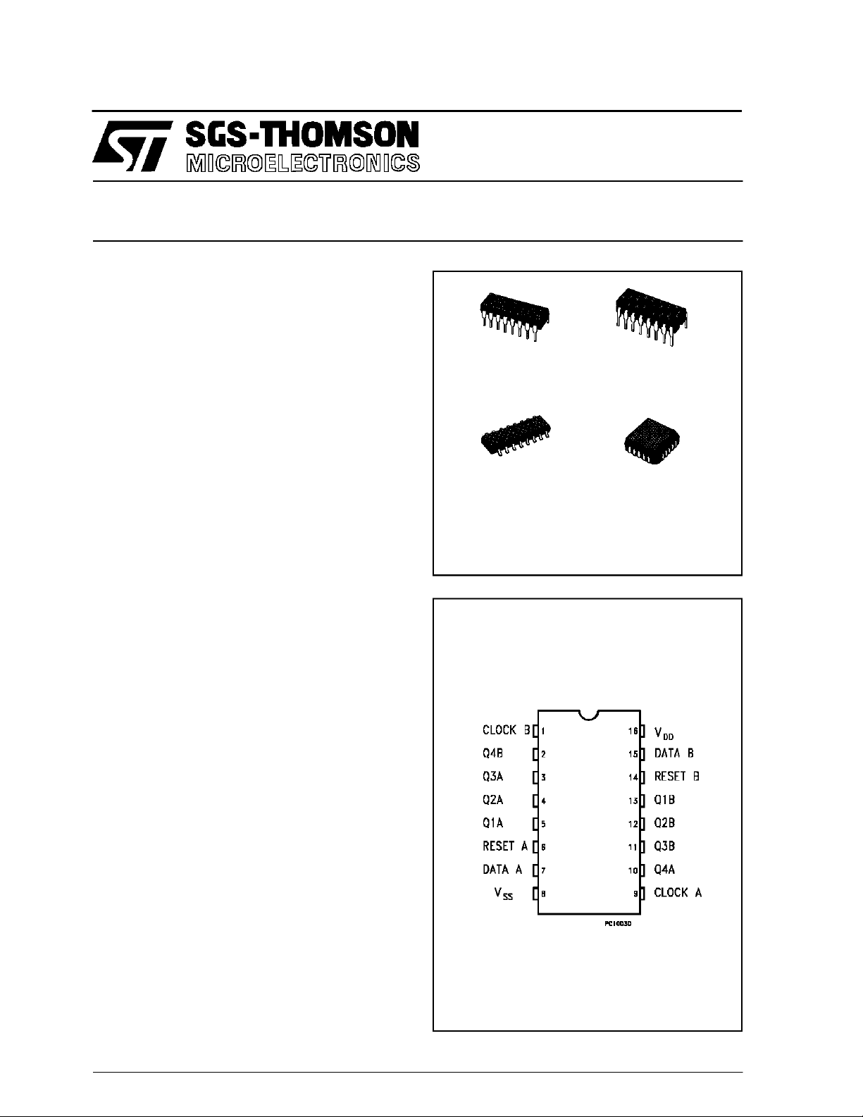
EY
(Plastic Package)F(Ceramic Frit Seal Package)
M1
(MicroPackage)
ORDERCODES :
HCC4015BF HCF4015BM1
HCF4015BEY HCF4015BC1
(Plastic Chip Carrier)
C1
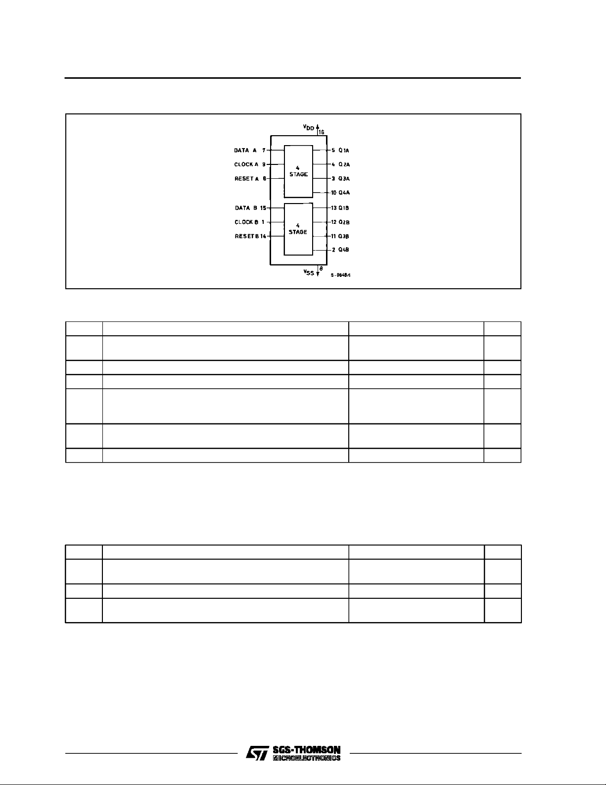
DESCRIPTION
TheHCC4015B(extended temperature range) and
HCF4015B (intermediate temperature range) are
monolithic integrated circuits, available in 16-lead
dual in-line plastic or ceramic package and plastic
micropackage.
TheHCC/HCF4015Bconsistsof two identical, inde-
pendent,4-stageserial-input/parallel-output registers.
Eachregister has independent CLOCK and RESET
inputsas well asa singleserialDATAinput. ”Q” outputsareavailablefromeachofthefourstagesonboth
registers.AllregisterstagesareD-type,master-slave
flip-flops. Thelogic level present attheDATA input is
transferredintothefirstregisterstageandshiftedover
onestageateach positive-going clocktransition. Resettingofallstagesisaccomplishedby ahighlevelon
the reset line. Register expansion to 8 stages using
one HCC/HCF4015B package, or to more than 8
stagesusingadditionalHCC/HCF4015B’sispossible.
PIN CON NECTIONS
June 1989
1/12
HCC/HCF4015B
FUNCTIONAL DIAGRAM
ABSOLUTE MAXIMU M RA TI NGS
Symbol Parame ter Val ue Unit
V
* Supply Voltage : HCC Types
DD
HCF Types
V
Input Voltage – 0.5 to VDD+ 0.5 V
i
I
DC Input Current (any one input) ± 10 mA
I
P
Total Power Dissipation (per package)
tot
Dissipation per Output Transistor
for T
T
Operating Temperature : HCC Types
op
= Full Package-temperature Range
op
HCF Types
T
Stresses above those listed under ”Absolute Maximum Ratings ”may cause permanent damage to the device. This is a stress
rating only and functional operation of the device at these or any other conditions above those indicated in the operational sections of this specification is not implied. Exposure to absolute maximum rating conditions for external periods may affect device
reliability.
* All voltage values are referred to VSSpin voltage.
Storasge Temperature – 65 to + 150 °C
stg
– 0.5 to + 20
– 0.5 to + 18
200
100
–55to+125
–40to+85
V
V
mW
mW
°C
°C
RECOMMENDED OPERATING CONDITIONS
Symbol Parameter Value Unit
V
T
2/12
Supply Voltage : HCC Types
DD
HCF Types
V
Input Voltage 0 to V
I
Operating Temperature : HCC Types
op
HCF Types
3to18
3to15
DD
– 55 to + 125
–40to+85
V
V
V
°C
°C
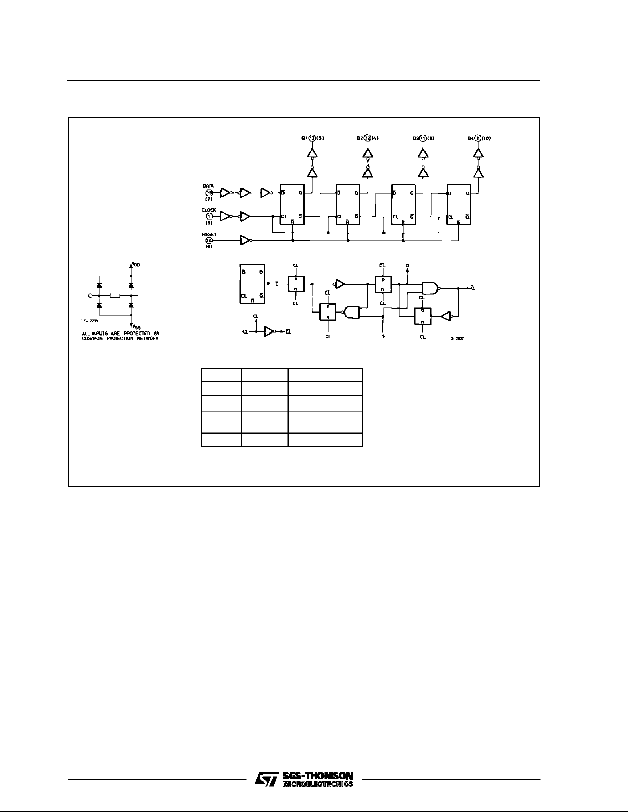
LOGIC DIAGRAMS AND TRUTH TABLE
HCC/HCF4015B
CL D R Q
–
/
–
–
–
000 Q
–
/
101 Q
X0Q
\
–
1
1
(no. change)
Q
n
n–1
n–1
Qn–
XX10 0
3/12
HCC/HCF4015B
STATIC ELECTRICAL CHARACTERISTICS (overrecommended operating conditions)
Test Conditions Value
Symbol Parameter
Quiescent
I
L
Current
HCC
Types
HCF
Types
V
OH
Output High
Voltage
V
OL
Output Low
Voltage
V
IH
Input High
Voltage
V
IL
Input Low
Voltage
I
OH
Output
Drive
Current
HCC
Types
HCF
Types
I
OL
Output
Sink
Current
HCC
Types
HCF
Types
I
IH,IIL
Input
Leakage
Current
HCC
Types
HCF
Types
C
Input Capacitance Any Input 5 7.5 pF
I
*T
=–55°CforHCC device : – 40°CforHCF device.
Low
*T
=+125°C for HCC device : + 85°C for HCF device.
High
The NoiseMargin forboth ”1” and ”0” level is: 1V min.with VDD=5V, 2V min.with VDD= 10V,2.5 V min.with VDD= 15V.
V
V
O
|IO|V
I
(V) (V) (µA) (V)
DD
T
* 25° CT
Low
Min. Max. Min. Typ. Max. Min. Max.
0/ 5 5 5 0.04 5 150
0/10 10 10 0.04 10 300
0/15 15 20 0.04 20 600
0/20 20 100 0.08 100 3000
0/ 5 5 20 0.04 20 150
0/10 10 40 0.04 40 300
0/15 15 80 0.04 80 600
0/ 5 < 1 5 4.95 4.95 4.95
0/10 < 1 10 9.95 9.95 9.95
0/15 < 1 15 14.95 14.95 14.95
5/0 < 1 5 0.05 0.05 0.05
10/0 < 1 10 0.05 0.05 0.05
15/0 < 1 15 0.05 0.05 0.05
0.5/4.5 < 1 5 3.5 3.5 3.5
1/9 < 1 10 7 7 7
1.5/13.5 < 1 15 11 11 11
4.5/0.5 < 1 5 1.5 1.5 1.5
9/1 < 1 10 3 3 3
13.5/1.5 < 1 15 4 4 4
0/ 5 2.5 5 – 2 – 1.6 – 3.2 –1.15
0/ 5 4.6 5 – 0.64 – 0. 51 –1 –0.36
0/10 9.5 10 – 1.6 – 1.3 – 2.6 – 0.9
0/15 13.5 15 – 4.2 – 3.4 – 6.8 – 2.4
0/ 5 2.5 5 – 1.53 – 1. 36 –3.2 –1.1
0/ 5 4.6 5 – 0.52 – 0.44 –1 –0.36
0/10 9.5 10 – 1.3 – 1.1 – 2.6 – 0.9
0/15 13.5 15 – 3.6 – 3.0 – 6.8 – 2.4
0/ 5 0.4 5 0.64 0.51 1 0.36
0/10 0.5 10 1.6 1.3 2.6 0.9
0/15 1.5 15 4.2 3.4 6.8 2.4
0/ 5 0.4 5 0.52 0.44 1 0.36
0/10 0.5 10 1.3 1.1 2.6 0.9
0/15 1.5 15 3.6 3.0 6.8 2.4
0/18
Any Input
0/15 15 ± 0.3 ±10
18 ± 0.1 ±10–5± 0. 1 ± 1
–5
± 0. 3 ± 1
High
Unit
*
µA
V
V
V
V
mA
mA
µA
4/12

HCC/HCF4015B
DYNAMIC ELECTRICAL CHARACTERISTICS (T
=25°C, CL= 50 pF, RL= 200kΩ,
amb
typical temperature coefficient forall VDDvalues is 0.3 %/°C, all inputrise and fall times = 20ns)
Symbol Paramet e r
Test Conditions
V
(V) Min. Typ. Max.
DD
CLOCKED OPERATION
t
PLH,tPHL
Propagation Delay Time
(carry out or decoded out lines)
5160320
10 80 160
15 60 120
t
THL,tTLH
Transition Time
(carry out or decoded out lines)
5100200
10 50 100
15 40 80
f
CL
Maximum Clock Input Frequency 5 3 6
10 6 12
15 8.5 17
t
Clock Pulse Width 5 180 90
W
10 80 40
15 50 25
t
* Clock Input Rise or Fall Time 5 15
r,tf
10 15
15 15
t
se tu p
Data Setup Time 5 70 35
10 40 20
15 30 15
RESET OPERATION
t
PLH,tPHL
Propagation Delay Time 5 200 400
10 100 200
15 80 160
t
Reset Pulse Width 5 200 100
W
10 80 40
15 60 30
* Ifmorethan unitis cascaded inthe parallelclocked application, trCLshould bemade less thanorequal tothe sumof thefixed propagation delay
at 15pFand the transition time of the carry output driving stagefor the estimated capacitive load.
Value
Unit
ns
ns
MHz
ns
µs
ns
ns
ns
5/12

HCC/HCF4015B
TypicalOutputLow (sink)Current Characteristics. MinimumOutputLow(sink)CurrentCharacteristics.
Typical Output High (source) Current Characteristics.
TypicaltransitionTime vs. LoadCapacitance.
Minimum Output High (source) Current Characteristics.
Typical propagation Delay Time vs. Load Capacitance..
6/12

TypicalDynamic PowerDissipation vs. Frequency.
TEST CIRCUITS
HCC/HCF4015B
QuiescentDevice Current.
Input Voltage.
Input current.
Power Dissipation.
7/12

HCC/HCF4015B
Plastic DIP16 (0.25) MECHANICAL DATA
DIM.
MIN. TYP. MAX. MIN. TYP. MAX.
a1 0.51 0.020
B 0.77 1.65 0.030 0.065
b 0.5 0.020
b1 0.25 0.010
D 20 0.787
E 8.5 0.335
e 2.54 0.100
e3 17.78 0.700
F 7.1 0.280
I 5.1 0.201
L 3.3 0.130
Z 1.27 0.050
mm inch
8/12
P001C

Ceramic DIP16/1 MECHANICAL DATA
HCC/HCF4015B
DIM.
MIN. TYP. MAX. MIN. TYP. MAX.
A 20 0.787
B 7 0.276
D 3.3 0.130
E 0.38 0.015
e3 17.78 0.700
F 2.29 2.79 0.090 0.110
G 0.4 0.55 0.016 0.022
H 1.17 1.52 0.046 0.060
L 0.22 0.31 0.009 0.012
M 0.51 1.27 0.020 0.050
N 10.3 0.406
P 7.8 8.05 0.307 0.317
Q 5.08 0.200
mm inch
P053D
9/12

HCC/HCF4015B
SO16 (Narrow) MECHANICAL DATA
DIM.
MIN. TYP. MAX. MIN. TYP. MAX.
A 1.75 0.068
a1 0.1 0.2 0.004 0.007
a2 1.65 0.064
b 0.35 0.46 0.013 0.018
b1 0.19 0.25 0.007 0.010
C 0.5 0.019
c1 45° (typ.)
D 9.8 10 0.385 0.393
E 5.8 6.2 0.228 0.244
e 1.27 0.050
e3 8.89 0.350
F 3.8 4.0 0.149 0.157
G 4.6 5.3 0.181 0.208
L 0.5 1.27 0.019 0.050
M 0.62 0.024
S8°(max.)
mm inch
10/12
P013H

PLCC20 MECHANICAL DATA
HCC/HCF4015B
DIM.
MIN. TYP. MAX. MIN. TYP. MAX.
A 9.78 10.03 0.385 0.395
B 8.89 9.04 0.350 0.356
D 4.2 4.57 0.165 0.180
d1 2.54 0.100
d2 0.56 0.022
E 7.37 8.38 0.290 0.330
e 1.27 0.050
e3 5.08 0.200
F 0.38 0.015
G 0.101 0.004
M 1.27 0.050
M1 1.14 0.045
mm inch
P027A
11/12

HCC/HCF4015B
Information furnished is believed tobe accurate and reliable.However, SGS-THOMSON Microelectronics assumes no responsability for the
consequences of use of such information nor for any infringementof patents or other rights of third parties which may results from its use. No
license isgranted by implicationor otherwise underany patent or patentrights of SGS-THOMSON Microelectronics.Specificationsmentioned
in this publication are subject to changewithout notice. This publication supersedes andreplaces all information previously supplied.
SGS-THOMSON Microelectronicsproductsare notauthorizedforuse ascritical componentsin life supportdevices orsystems withoutexpress
written approval of SGS-THOMSON Microelectonics.
1994 SGS-THOMSON Microelectronics - All RightsReserved
Australia - Brazil - France - Germany - Hong Kong - Italy - Japan - Korea - Malaysia - Malta - Morocco - The Netherlands -
Singapore - Spain - Sweden - Switzerland - Taiwan - Thailand - United Kingdom - U.S.A
SGS-THOMSON MicroelectronicsGROUP OF COMPANIES
12/12
 Loading...