

HCC/H CF4 01 4B
HCC/HCF4021B
8-STAGESTATIC SHIFT REGISTERS
4014B SYNCHRONOUS PARALLEL OR
SERIAL INPUT/SERIAL OUTPUT
4021B ASYNCHRONOUS PARALLEL
INPUT OR SYNCHRONOUS
SERIAL INPUT/SERIAL OUTPUT
. MEDIUM-SPEED OPERATION-12MHz (typ.)
CLOCKRATE AT VDD–VSS=10V
.FULLYSTATIC OPERATION
.8 MASTER-SLAVE FLIP-FLOPS PLUS OUT-
PUT BUFFERING AND CONTROL GATING
.QUIESCENT CURRENT SPECIFIED TO 20V
FOR HCC DEVICE
.5V, 10V AND 15V PARAMETRIC RATINGS
.INPUT CURRENTOF 100nA AT 18V AND25°C
FOR HCC DEVICE
.100% TESTEDFOR QUIESCENTCURRENT
.MEETSALLREQUIREMENTSOFJEDECTEN-
TATIVE STANDARD No13A, ”STANDARD
SPECIFICATIONS FOR DESCRIPTION OF ”B”
SERIESCMOS DEVICES”
DESCRI PTIO N
TheHCC4014B, HCC4021B (extended temperatu-
re range)and theHCF4014B, HCF4021B (interme-
diate temperature range) are monolithic integrated
circuits,available in16-leaddual in-line plasticorceramic package and plastic micro package. The
HCC/HCF4014BandHCC/HCF4021B seriestypes
are 8-stage parallel-or serial-input/serial-output registers having common CLOCK and PARALLEL/SERIAL CONTROL inputs, a single SERIAL
data input, and individual parallel ”JAM” inputs to
eachregister stage. Each register stageisa Dtype,
master-slave flip-flop in addition to an output from
stage 8, ”Q” outputsare alsoavailable fromstages
6 and7. Parallel as well as serial entry ismade into
the registersynchronously withthe positiveclockline transition in the HCC/HCF4014B. In the
HCC/HCF4021B serial entry is synchronous with
the clock butparallel entry is asynchronous. In both
types,entryis controlled bythePARALLEL/SERIAL
CONTROL input. When the PARALLEL/SERIAL
CONTROL inputis low, data is serially shifted into
the 8-stage register synchronously with thepositive
transition of the clock line. When the PARALLEL/SERIAL CONTROL input is high,data is jammed into the 8-stage register via the parallel input
lines and synchronous withthepositive transition of
the clockline. In the HCC/HCF4021B, the CLOCK
inputof theinternal stageis ”forced” whenasynchronous parallel entry is made. Register expansion
usingmultiple packageis permitted.
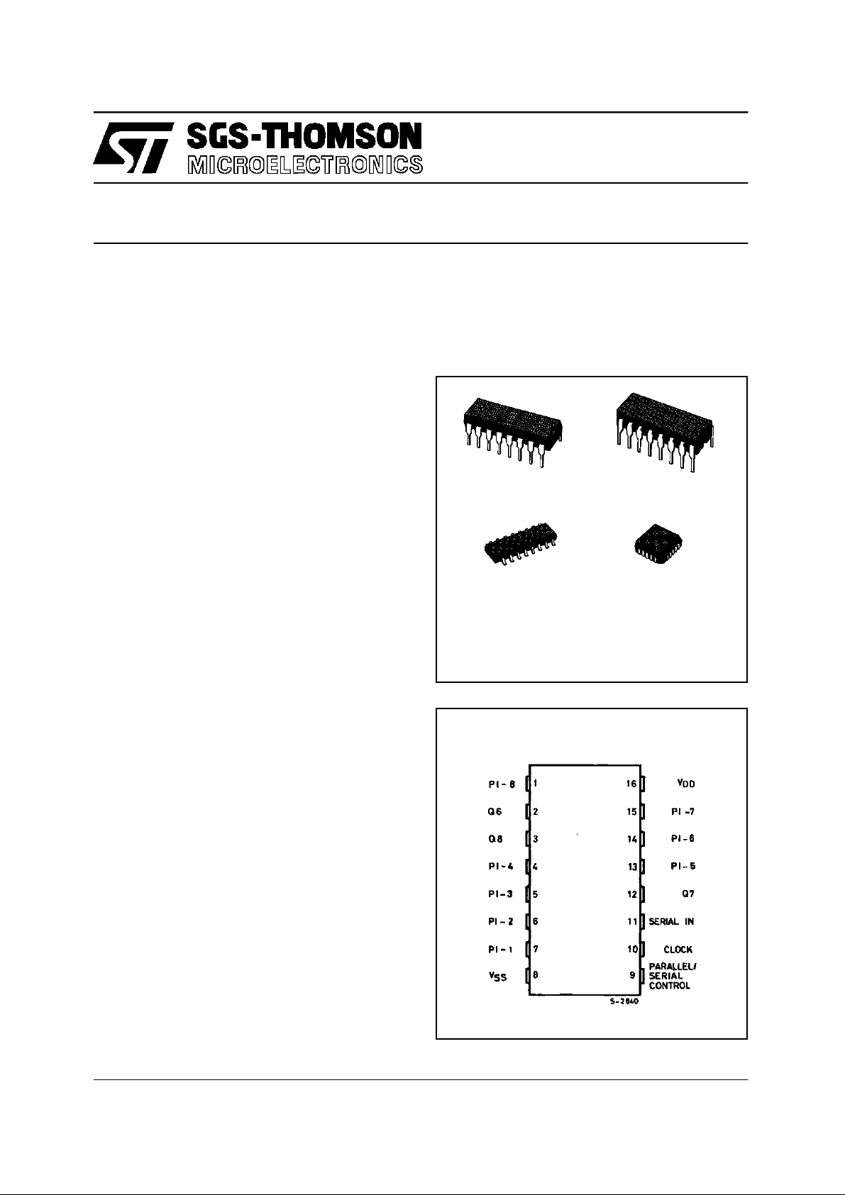
EY
(Plastic Package)
M1
(MicroPackage)
ORDERCODES :
HCC40XXBF HCF40XXBM1
HCF40XXBE Y HCF40XXBC1
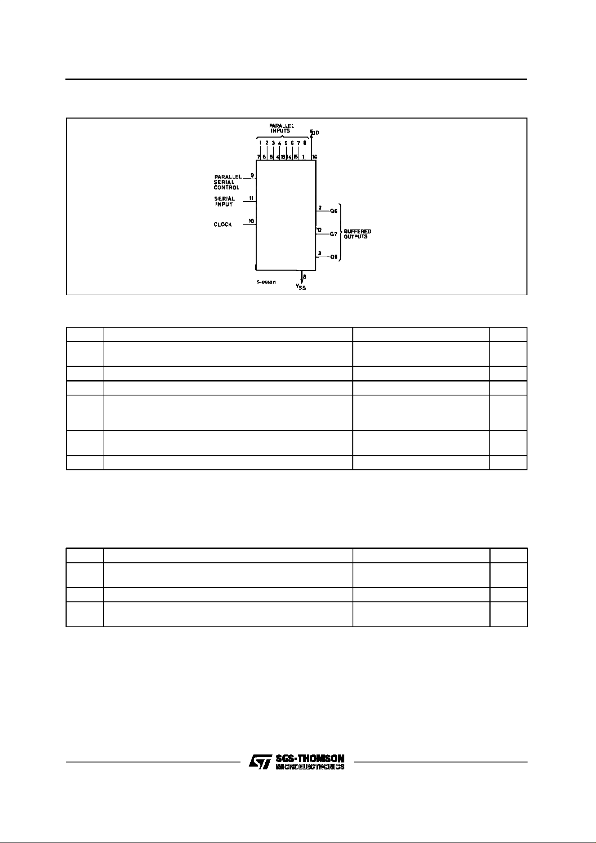
PIN CONNECTION S
(Ceramic Package)
(Plastic Chip Carrier)
F
C1
November1996
1/13
HCC/HCF4014B/4021B
FUN CTIONAL DIAGRA M
ABSOLUTE MAXIMU M RA TINGS
Symbol Parameter Val ue Unit
V
* Supply Voltage : HCC Types
DD
HCF Types
V
Input Voltage – 0.5 to VDD+ 0.5 V
i
I
DC Input Current (any one input) ± 10 mA
I
P
Total Power Dissipation (per package)
tot
Dissipation per Output Transistor
for T
T
Operating Temperature : HCC Types
op
= Full Package-temperature Range
op
HCF Types
T
Stresses above those listed under ”Absolute MaximumRatings”may cause permanent damage tothe device. This is a stressrating onlyand
functionaloperation of the deviceat theseor any otherconditionsabove those indicated inthe operational sectionsof this specificationis not
implied.Exposure toabsolute maximum ratingconditionsfor external periods may affectdevice reliability.
*
Allvoltage values arereferredto VSSpinvoltage.
Storage Temperature – 65 to + 150 °C
stg
– 0.5to + 20
– 0.5to + 18
200
100
–55to+125
–40to+85
V
V
mW
mW
°C
°C
RECOMMENDED OPERATING CONDITIONS
Symbol Parameter Value Unit
V
T
2/13
Supply Voltage : HCC Types
DD
HCF Types
V
Input Voltage 0 to V
I
Operating Temperature : HCC Types
op
HCF Types
3to18
3to15
DD
– 55 to + 125
–40to+85
V
V
V
°C
°C
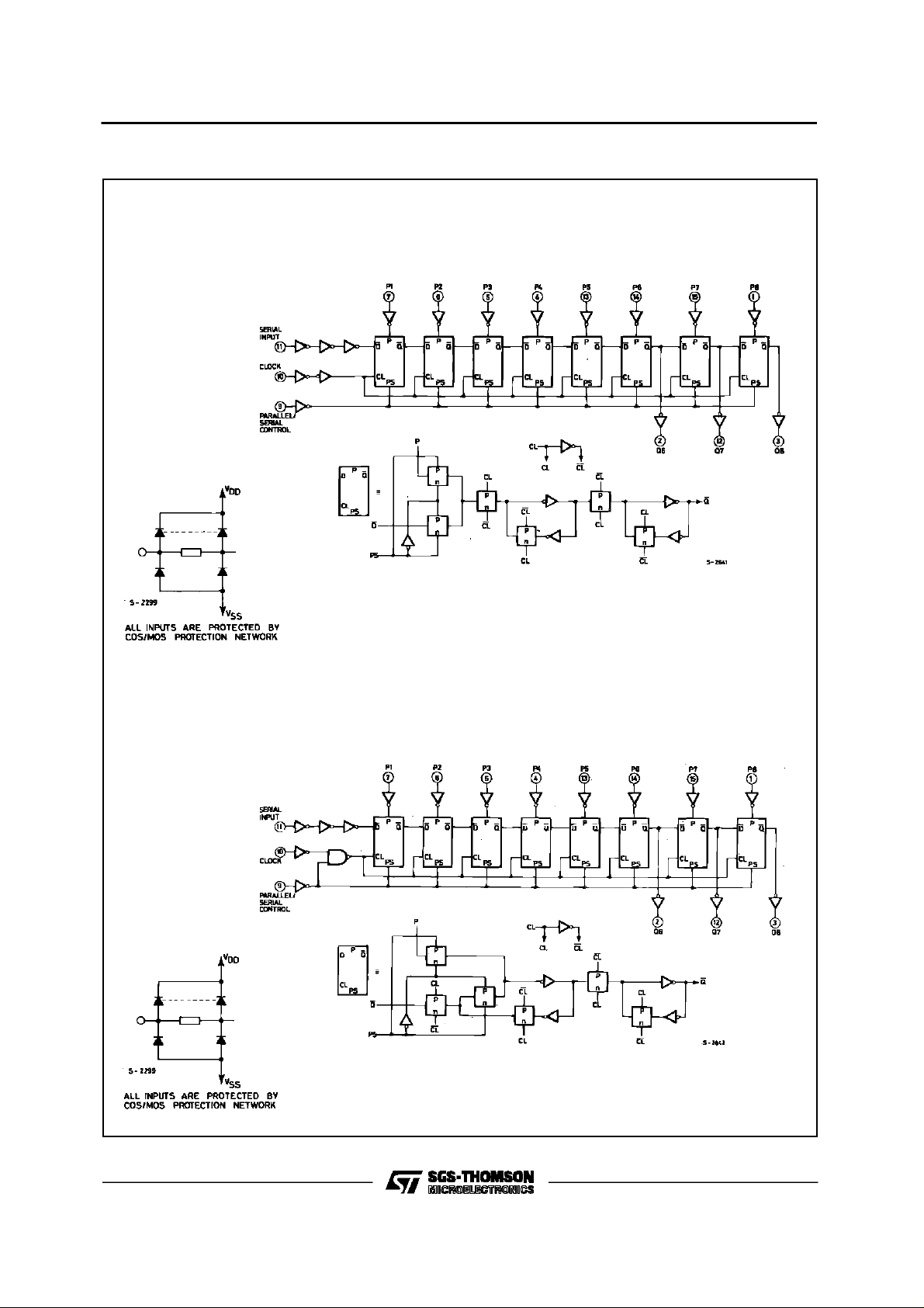
LOGIC DI AGRAMS
4014B
HCC/HCF4014B/4021B
4021B
3/13
HCC/HCF4014B/4021B
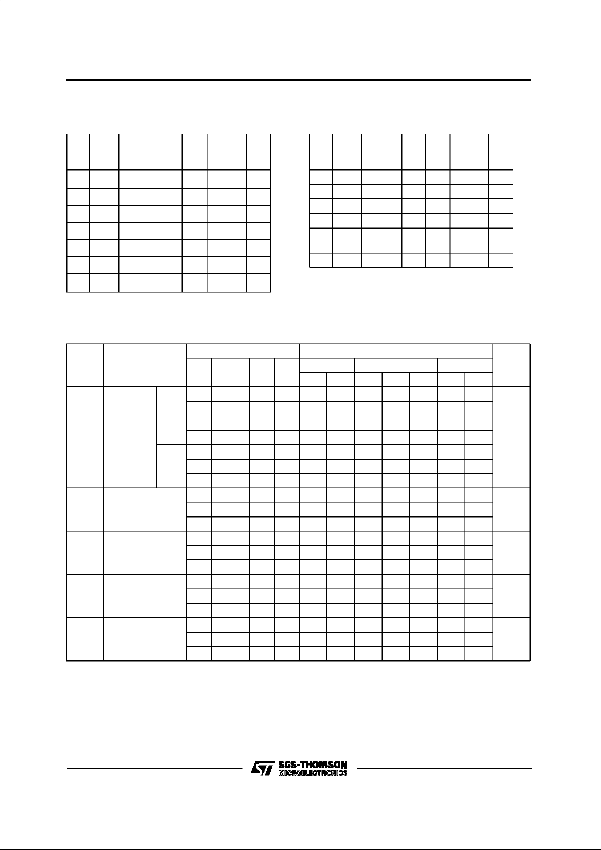
TRUTH TABLES
HCC/HCF4014B
Parallel/
Serial
CL
Input
–
/
–
–
/
–
–
/
–
–
/
–
–
/
–
–
/
–
–
\
–
X = don’t care case.
NC = no change.
Seri al
Control
X10000
X11010
X10101
X11111
00XX0Q
10XX1Q
XXXXQ
Pl–1 Pl–n
Q
1
(internal)
1
Q
n
–1
n
I
–1
n
Q
NC
n
HCC/HCF4021B
Parallel/
Seri al
CL
Input
Serial
Control
XX 1 00 0 0
XX 1 01 0 1
XX 1 10 1 0
XX 1 11 1 1
–
0
/
–
1
–
\
X0XXQ
–
X = don’t care case.
NC = nochange.
0
0
Pl–1 Pl–n
X
X
X
X
STATIC ELECTRICAL CHARACTERISTICS (overrecommended operating conditions)
Test Condi t io n s Value
Symbol Parameter
(V) (V) (µA) (V)
I
L
Quiescent
Current
HCC
Types
0/ 5 5 5 0.04 5 150
0/10 10 10 0.04 10 300
0/15 15 20 0.04 20 600
0/20 20 100 0.08 100 3000
0/ 5 5 20 0.04 20 150
HCF
Types
0/10 10 40 0.04 40 300
0/15 15 80 0.04 80 600
V
OH
Output High
Voltage
0/ 5 < 1 5 4.95 4.95 4.95
0/10 < 1 10 9.95 9.95 9.95
0/15 < 1 15 14.95 14.95 14.95
V
OL
Output Low
Voltage
5/0 < 1 5 0.05 0.05 0.05
10/0 < 1 10 0.05 0.05 0.05
15/0 < 1 15 0.05 0.05 0.05
V
IH
Input High
Voltage
V
IL
Input Low
Voltage
*T
=–55°CforHCC device: – 40°C for HCF device.
Low
*T
= +125°C forHCC device: + 85°C forHCF device.
High
TheNoise Margin for both”1” and”0” levelis : 1V min.with VDD=5V, 2V min.withVDD= 10V,2.5 V min.with VDD= 15V.
V
V
I
O
|IO|V
DD
T
* 25°CT
Low
Min. Max. Min. Typ. Max. Min. Max.
0.5/4.5 < 1 5 3.5 3.5 3.5
1/9 < 1 10 7 7 7
1.5/13.5 < 1 15 11 11 11
4.5/0.5 < 1 5 1.5 1.5 1.5
9/1 < 1 10 3 3 3
13.5/1.5 < 1 15 4 4 4
Q
1
(internal)
0
1
1
*
High
Q
n
Q
–1
n
Qn–1
Q
n
Unit
µA
V
V
V
V
I
NC
4/13

HCC/HCF4014B/4021B
STATIC ELECTRICAL CHARACTERISTICS (continued)
Test Conditions Valu e
Symbol Parameter
I
OH
Output
Drive
Current
HCC
Types
HCF
Types
I
OL
Output
Sink
Current
HCC
Types
HCF
Types
I
IH,IIL
Input
Leakage
Current
HCC
Types
HCF
Types
C
Input Capacitance Any Input 5 7.5 pF
I
*T
=–55°CforHCC device: – 40°C for HCF device.
Low
*T
= +125°C forHCC device: + 85°C forHCF device.
High
TheNoise Margin for both”1” and”0” levelis : 1V min.with VDD=5V, 2V min.withVDD= 10V,2.5 V min.with VDD= 15V.
V
V
O
|IO|V
I
(V) (V) (µA) (V)
T
DD
* 25°CT
Low
Min. Max. Min. Typ. Max. Min. Max.
0/ 5 2.5 5 – 2 – 1.6 – 3.2 – 1.15
0/ 5 4.6 5 – 0.64 – 0.51 – 1 – 0.36
0/10 9.5 10 – 1.6 – 1.3 – 2.6 – 0.9
0/15 13.5 15 – 4.2 – 3.4 – 6.8 – 2.4
0/ 5 2.5 5 – 1.53 – 1.36 – 3.2 – 1.1
0/ 5 4.6 5 – 0.52 – 0.44 – 1 – 0.36
0/10 9.5 10 – 1.3 – 1.1 – 2.6 – 0.9
0/15 13.5 15 – 3.6 – 3.0 – 6.8 – 2.4
0/ 5 0.4 5 0.64 0.51 1 0.36
0/10 0.5 10 1.6 1.3 2.6 0.9
0/15 1.5 15 4.2 3.4 6.8 2.4
0/ 5 0.4 5 0.52 0.44 1 0.36
0/10 0.5 10 1.3 1.1 2.6 0.9
0/15 1.5 15 3.6 3.0 6.8 2.4
0/18
Any Input
0/15 15 ± 0.3 ±10
18 ± 0.1 ±10–5± 0.1 ± 1
–5
± 0.3 ± 1
High
Unit
*
mA
mA
µA
DYNAMIC ELECTRICAL CHARACTERISTICS (T
=25°C, CL= 50pF, RL= 200kΩ,
amb
typical temperature coefficient forall VDD= 0.3%/°C values, all input rise and fall time = 20ns)
Symbol Par amet e r
Test Conditions
V
(V) Min. Typ. Ma x.
DD
CLOCKED OPERATION
t
PLH,tPHL
Propagation Delay Time 5 160 320
10 80 160
15 60 120
t
THL,tTLH
Transition Time 5 100 200
10 50 100
15 40 80
f
* Maximum Clock Input Frequency 5 3 6
CL
10 6 12
15 8.5 17
t
Clock Pulse Width 5 180 90
W
10 80 40
15 50 25
*
If more thanone unitis cascaded trCL shouldbe made less thanor equal to thesum of the transition time and thefixed propagation delay of
the outputof the driving stageof the estimated capacitive load.
Value
Unit
MHz
ns
ns
ns
5/13

HCC/HCF4014B/4021B
DYNAMIC ELECTRICAL CHARACTERISTICS (Con tinued)
Symbol Parameter
Test Conditions Value
(V) Min. Typ. Max.
V
DD
Unit
CLOCKED OPERATION
t
Clock Input Rise or Fall Time 5 15
r,tf
10 15
15 15
t
setup
Setup Time, serial Input (ref. to CL) 5 120 60
10 80 40
15 60 30
t
setup
Setup Time, parallel Input (4014B)
(ref. to CL)
58040
10 50 25
15 40 20
t
setup
Setup Time, parallel Input (4021B)
(ref. to P/S)
55025
10 30 15
15 20 10
t
setup
Setup Time, parallel/serial Control (4014B)
(ref. to CL)
5 180 90
10 80 40
15 60 30
t
Hold Time, serial in, parallel in,
hold
parallel/serial Cotrol
50
10 0
15 0
t
P/S Pulse Width (4021B) 5 160 80
WH
10 80 40
15 50 25
t
P/S Removal time (4021B)
rem
(ref. to CL)
5 280 140
10 140 70
15 100 50
*
If more thanone unitis cascaded trCL shouldbe made less thanor equal to thesum of the transition time and thefixed propagation delay of
the outputof the driving stageof the estimated capacitive load.
µs
ns
ns
ns
ns
ns
ns
ns
TypicalOutput Low (sink) Current Characteristics. Minimum Output Low(sink) Current Charac-
teristics.
6/13

HCC/HCF4014B/4021B
TypicalOutput High (source) CurrentCharacteristics.
Minimum Output High (source) Current Characteristics.
TypicalTransition Timevs. Load Capacitance. Typical Propagation Delay Time vs.Load Capacit-
ance.
TypicalDynamic PowerDissapating vs.Clock
Input Frequency.
7/13

HCC/HCF4014B/4021B
TEST CIRCUITS
QuiescentDevice Current.
Noise Immunity.
Input Leakage Current. DynamicPower Dissipation.
8/13

HCC/HCF4014B/4021B
Plastic DIP16 (0.25) MECHANICAL DATA
DIM.
MIN. TYP. MAX. MIN. TYP. MAX.
a1 0.51 0.020
B 0.77 1.65 0.030 0.065
b 0.5 0.020
b1 0.25 0.010
D 20 0.787
E 8.5 0.335
e 2.54 0.100
e3 17.78 0.700
F 7.1 0.280
I 5.1 0.201
L 3.3 0.130
Z 1.27 0.050
mm inch
P001C
9/13

HCC/HCF4014B/4021B
Ceramic DIP16/1 MECHANICAL DATA
DIM.
MIN. TYP. MAX. MIN. TYP. MAX.
A 20 0.787
B 7 0.276
D 3.3 0.130
E 0.38 0.015
e3 17.78 0.700
F 2.29 2.79 0.090 0.110
G 0.4 0.55 0.016 0.022
H 1.17 1.52 0.046 0.060
L 0.22 0.31 0.009 0.012
M 0.51 1.27 0.020 0.050
N 10.3 0.406
P 7.8 8.05 0.307 0.317
Q 5.08 0.200
mm inch
10/13
P053D

SO16 (Narrow) MECHANICAL DATA
HCC/HCF4014B/4021B
DIM.
MIN. TYP. MAX. MIN. TYP. MAX.
A 1.75 0.068
a1 0.1 0.2 0.004 0.007
a2 1.65 0.064
b 0.35 0.46 0.013 0.018
b1 0.19 0.25 0.007 0.010
C 0.5 0.019
c1 45° (typ.)
D 9.8 10 0.385 0.393
E 5.8 6.2 0.228 0.244
e 1.27 0.050
e3 8.89 0.350
F 3.8 4.0 0.149 0.157
G 4.6 5.3 0.181 0.208
L 0.5 1.27 0.019 0.050
M 0.62 0.024
S8°(max.)
mm inch
P013H
11/13

HCC/HCF4014B/4021B
PLCC20 MECHANICAL DATA
DIM.
MIN. TYP. MAX. MIN. TYP. MAX.
A 9.78 10.03 0.385 0.395
B 8.89 9.04 0.350 0.356
D 4.2 4.57 0.165 0.180
d1 2.54 0.100
d2 0.56 0.022
E 7.37 8.38 0.290 0.330
e 1.27 0.050
e3 5.08 0.200
F 0.38 0.015
G 0.101 0.004
M 1.27 0.050
M1 1.14 0.045
mm inch
12/13
P027A

HCC/HCF4014B/4021B
Information furnished is believed to be accurate and reliable. However, SGS-THOMSON Microelectronics assumes no responsability for the
consequences of useof such information nor for any infringement of patents or other rights of third parties which may results from its use.No
licenseis granted by implication or otherwise under any patent or patent rights of SGS-THOMSONMicroelectronics. Specifications mentioned
in thispublication aresubject to change withoutnotice. Thispublication supersedes andreplacesall informationpreviously supplied.
SGS-THOMSONMicroelectronics products are notauthorized for use ascriticalcomponents in lifesupport devices or systems without express
writtenapproval ofSGS-THOMSONMicroelectonics.
1996 SGS-THOMSONMicroelectronics - Printedin Italy- All Rights Reserved
Australia- Brazil - Canada - China - France- Germany - HongKong- Italy - Japan- Korea- Malaysia - Malta - Morocco- The Netherlands-
Singapore - Spain- Sweden- Switzerland - Taiwan - Thailand- UnitedKingdom - U.S.A
SGS-THOMSONMicroelectronics GROUPOF COMPANIES
.
13/13
 Loading...