

10 TO 4 LINEBCD PRIORITY ENCODER
.ENCODES 10 LINE TO 4 LINEBCD
.ACTIVELOW INPUTSAND OUTPUTS
.STANDARDIZED, SYMMETRICAL OUTPUT
CHARACTERIZATION
.100 % TESTEDFOR QUIESCENT CURRENT
AT 20V
.5V, 10VAND 15VPARAMETRIC RATINGS
.MAXIMUMINPUTCURREENTOF 1µA AT18V
OVER FULL PACKAGE TEMPERATURE
RANGE;100 nA AT 18 VAND 25oC
.NOISE MARGIN (FULL PACKAGE TEMPERA-
TURERANGE): 1V AT VDD=5V, 2V AT
VDD=10V, 2.5VAT VDD= 15V
APPLICATIONS:
.KEYBOARD ENCODING
.10 LINE TO BCD ENCODING
.RANGE SELECTION
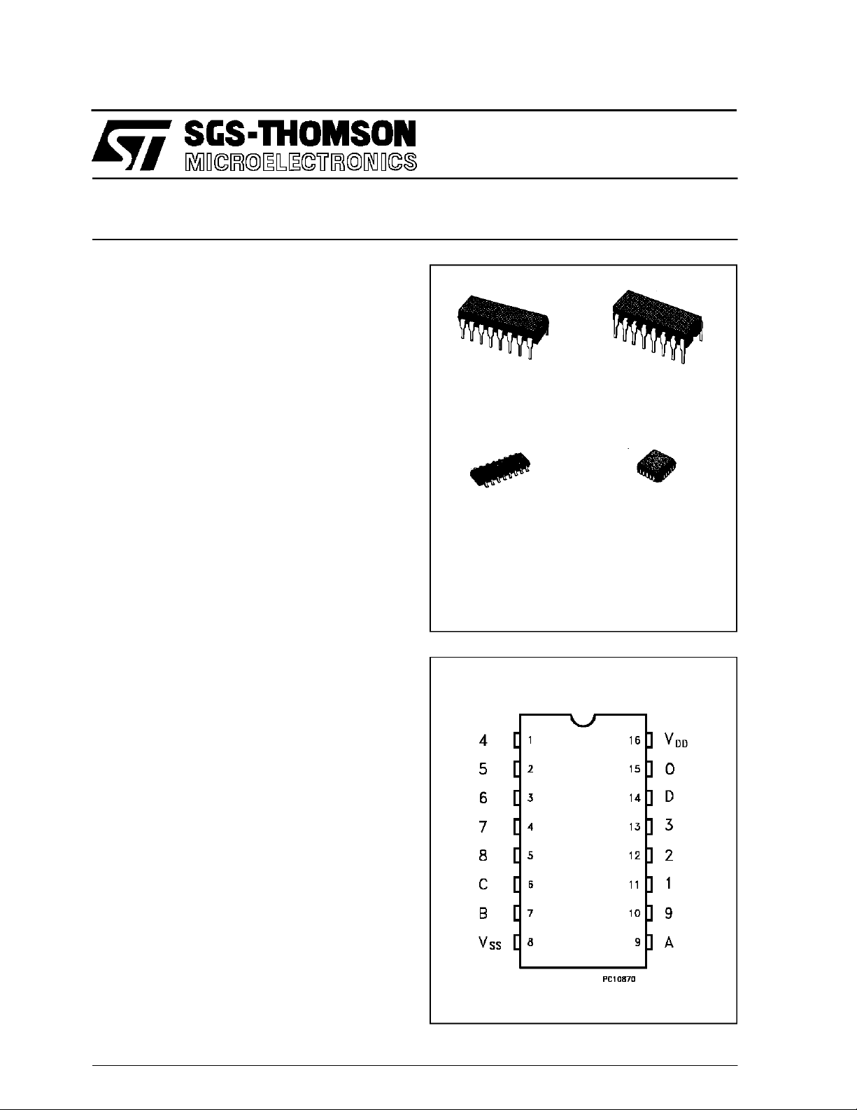
EY
(PlasticPackage)
M1
(MicroPackage)
HCC40147B
HCF 401 47 B
F
(CeramicPackage)
C1
(Chip Carrier)
DESCRIPT ION
The HCC/HCF40147B CMOS encoder features
priority encodingoftheinputstoensure thatonlythe
highest order data line is encoded. Ten data input
lines (0-9) are encoded to fourline (8, 4, 2, 1) BCD.
The highestpriority lineisline 9.Allfouroutputlines
arelogic 1 (VSS) when all input lines are logic0.All
inputs and outputs are buffered, and each output
can drive one TTL Low Power Schottky load. The
HCC/HCFF40147 is functionally similar to the
T54/T74LS147 if pin 15 istied low.
TheHCC/HCF40147B typesaresupplied in16lead
plasticor ceramic andplastic micropackage.
ORDER CODES :
HCC4 0147BF HCF40147BM1
HCF40147BE Y HCF40147BC1
PIN CONNECTIONS
April1991
1/12
HCC/HCF40147B
ABSOLU TE MAXIMUM RATING
Symbol Parameter Value Unit
V
* Supply Voltage: HCC Types
DD
HCF Types
V
P
Input Voltage -0.5 to VDD+ 0.5 V
i
I
DC Input Current (any one input) ± 10 mA
I
Total Power Dissipation (per package)
tot
Dissipation per Output Transistor
for Top = Full Package Temperature Range
T
Operating Temperature: HCC Types
op
HCF Types
T
Stressesabove those listedunder ”Absolute Maximum Ratings”maycausepermanent damagetothedevice. Thisisastressratingonlyandfunctional
operationofthe device attheseor anyother conditionsabove thoseindicated intheoperationalsections of thisspecification isnot implied.Exposure
to absolute maximum rating conditions forexternal periods may affect device reliability.
* Allvoltagevalues arereferredto VSSpinvoltage.
Storage Temperature -65 to +150
stg
RECO MM ENDED OPERAT I N G C O NDITI ONS
Symbol Parameter Value Unit
V
V
T
Supply Voltage: HCC Types
DD
HCF Types
Input Voltage 0 to V
I
Operating Temperature: HCC Types
op
HCF Types
-0.5 to +20
-0.5 to +18
200
100
-55 to +125
-40 to +85
3to18
3to15
DD
-55 to +125
-40 to +85
V
V
mW
mW
o
C
o
C
o
C
V
V
V
o
C
o
C
TRUTH TABLE
INPUT OUTPUTS
0123456789DCBA
00000000001111
10000000000000
X1000000000001
XX100000000010
XXX10000000011
XXXX1000000100
XXXXX100000101
XXXXXX10000110
XXXXXXX1000111
XXXXXXXX1 01000
XXXXXXXXX11001
0 = HighLevel, 1 = LowLevel, X =Don’tCare
2/12
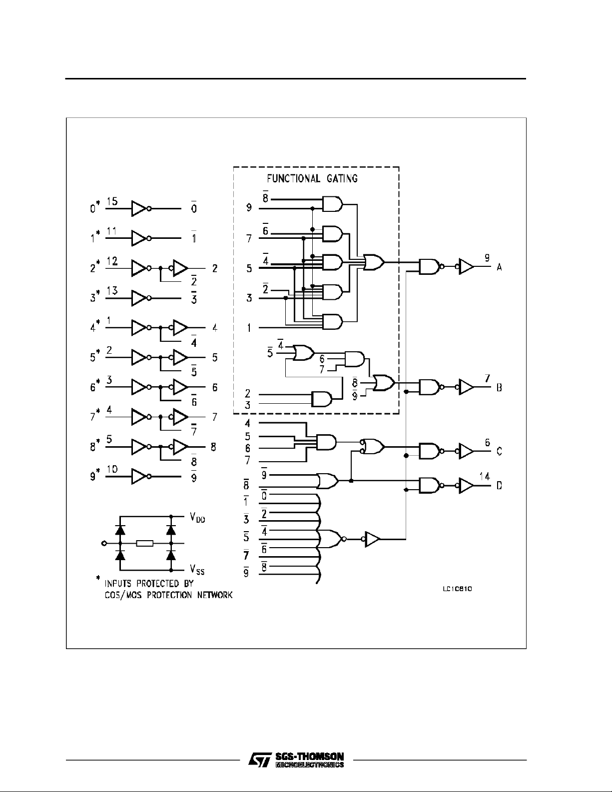
LOGI C DIAGRAM
HCC/HCF40147B
3/12
HCC/HCF40147B
STATI C ELECTRIC AL CHARACTER I STI CS (ove r recommended o perat i ng condit i o ns)
Test Conditios Value
Symbol Parameter
Quiescent
I
L
Current
HCC
Types
V
(V)
V
I
(V)
|IO|
(µA)
V
(V)
O
T
DD
*25
LOW
Min. Max. Min. Typ. Max. Min. Max.
0/5 5 1 0.02 1 30
0/10 10 2 0.02 2 60
0/15 15 4 0.02 4 120
o
CT
0/20 20 20 0.04 20 600
HCF
Types
0/5 5 4 0.02 4 30
0/10 10 8 0.02 8 60
0/15 15 16 0.02 16 120
OH
Output High
V
Voltage
0/5 < 1 5 4.95 4.95 4.95
0/10 < 1 10 9.95 9.95 9.95
0/15 < 1 15 14.95 14.95 14.95
OL
Output Low
V
Voltage
5/0 < 1 5 0.05 0.05 0.05
10/0 < 1 10 0.05 0.05 0.05
15/0 < 1 15 0.05 0.05 0.05
IH
Input High
V
Voltage
0.5/4.5 < 1 5 3.5 3.5 3.5
1/9 < 1 10 7 7 7
1.5/13.5 < 1 15 11 11 11
IL
Input Low
V
Voltage
4.5/0.5 < 1 5 1.5 1.5 1.5
9/1 < 1 10 3 3 3
13.5/1.5 < 1 15 4 4 4
OH
Output
Drive
Current
HCC
Types
I
0/5 2.5 5 -2 -1.6 -3.2 -1.15
0/5 4.6 5 -0.64 -0.51 -1 -0.36
0/10 9.5 10 -1.6 -1.3 -2.6 -0.9
0/15 13.5 15 -4.2 -3.4 -6.8 -2.4
0/5 2.5 5 -1.53 -1.36 -3.2 -1.1
HCF
Types
0/5 4.6 5 -0.52 -0.44 -1 -0.36
0/10 9.5 10 -1.3 -1.1 -2.6 -0.9
0/15 13.5 15 -3.6 -3.0 -6.8 -2.4
I
OL
Output
Sink
Current
HCC
Types
HCF
Types
0/5 0.4 5 0.64 0.51 1 0.36
0/10 0.5 10 1.6 1.3 2.6 0.9
0/15 1.5 15 4.2 3.4 6.8 2.4
0/5 0.4 5 0.52 0.44 1 0.36
0/10 0.5 10 1.3 1.1 2.6 0.9
0/15 1.5 15 3.6 3.0 6.8 2.4
I
IH,IIL
Input Leakage
Current
C
*T
LOW
*T
HIGH
TheNoise Marginfor both ”1” and”0” levelis: 1V min.withVDD=5 V, 2V min.with VDD=10 V, 2.5V min. withVDD=15V
Input Capacitance Any Input 5 7.5 pF
I
=-55oCforHCC device:-40oC forHCF device.
=+125oCforHCC device: +85oC for HCF device.
0/18
0/15 15 ±0.3 ±10
Any Input
18 ±0.1 ±10-5±0.1 ±1 µA
-5
±0.3 ±1 µA
HIGH
Unit
*
µA
V
V
V
V
mA
mA
4/12

HCC/HCF40147B
DYNAMIC ELECTRICAL CHARACTERISTICS (T
=25oC, CL=50pF,RL= 200 KΩ,
amb
typic al temperatur e coeff i c ent f or all VDDvalues is 03 %/oC, all input rise and fall t im es = 20 ns)
Symbol Parameter
t
t
t
t
t
t
PLH
PHL
PLH
PHL
TLH
THL
C
Propagation Delay Time
In Phase Output
Propagation Delay Time
Out of Phase Output
Transition Time 5 100 200
Input Capacitance 5 7.5 pF
I
Typical Output Low (source) Current Characteristics
Test Conditions Value
(V) Min. Typ. Max.
V
DD
Unit
5 450 900
10 200 400
ns
15 150 300
5 425 850
10 175 350
ns
15 125 250
10 50 100
ns
15 40 80
Minimum Output Low (source) Current Characteristics
Typical Output High (source) Current Characteristics
Minimum Output High (source) Current Characteristics
5/12

HCC/HCF40147B
Propagation Delay Time vs Load Capacitance Tipical Transition Time vs Load Capacitance
Typical Dynamic Power Dissipation vs Input Frequency
6/12

TEST CIRCUITS
QuiescentDevice Current. Noise Immunity.
HCC/HCF40147B
Input Leakage Current.
Dynamic Power DIssipation Test Circuit
7/12

HCC/HCF40147B
Plastic DIP16 (0.25) MECHANICAL DATA
DIM.
MIN. TYP. MAX. MIN. TYP. MAX.
a1 0.51 0.020
B 0.77 1.65 0.030 0.065
b 0.5 0.020
b1 0.25 0.010
D 20 0.787
E 8.5 0.335
e 2.54 0.100
e3 17.78 0.700
F 7.1 0.280
I 5.1 0.201
L 3.3 0.130
Z 1.27 0.050
mm inch
8/12
P001C

Ceramic DIP16/1 MECHANICAL DATA
HCC/HCF40147B
DIM.
MIN. TYP. MAX. MIN. TYP. MAX.
A 20 0.787
B 7 0.276
D 3.3 0.130
E 0.38 0.015
e3 17.78 0.700
F 2.29 2.79 0.090 0.110
G 0.4 0.55 0.016 0.022
H 1.17 1.52 0.046 0.060
L 0.22 0.31 0.009 0.012
M 0.51 1.27 0.020 0.050
N 10.3 0.406
P 7.8 8.05 0.307 0.317
Q 5.08 0.200
mm inch
P053D
9/12

HCC/HCF40147B
SO16 (Narrow) MECHANICAL DATA
DIM.
MIN. TYP. MAX. MIN. TYP. MAX.
A 1.75 0.068
a1 0.1 0.2 0.004 0.007
a2 1.65 0.064
b 0.35 0.46 0.013 0.018
b1 0.19 0.25 0.007 0.010
C 0.5 0.019
c1 45° (typ.)
D 9.8 10 0.385 0.393
E 5.8 6.2 0.228 0.244
e 1.27 0.050
e3 8.89 0.350
F 3.8 4.0 0.149 0.157
G 4.6 5.3 0.181 0.208
L 0.5 1.27 0.019 0.050
M 0.62 0.024
S8°(max.)
mm inch
10/12
P013H

PLCC20 MECHANICAL DATA
HCC/HCF40147B
DIM.
MIN. TYP. MAX. MIN. TYP. MAX.
A 9.78 10.03 0.385 0.395
B 8.89 9.04 0.350 0.356
D 4.2 4.57 0.165 0.180
d1 2.54 0.100
d2 0.56 0.022
E 7.37 8.38 0.290 0.330
e 1.27 0.050
e3 5.08 0.200
F 0.38 0.015
G 0.101 0.004
M 1.27 0.050
M1 1.14 0.045
mm inch
P027A
11/12

HCC/HCF40147B
Information furnished is believed to be accurate and reliable. However, SGS-THOMSON Microelectronics assumes no responsability for the
consequences of use of such information nor for any infringement of patents or other rights of third parties which may results from its use. No
license is grantedby implication or otherwise underany patentor patent rights of SGS-THOMSON Microelectronics. Specificationsmentioned
in this publication are subject to changewithout notice. This publication supersedes and replaces all information previously supplied.
SGS-THOMSON Microelectronicsproductsare notauthorized foruse ascritical componentsin life supportdevices or systemswithout express
written approval of SGS-THOMSON Microelectonics.
1994 SGS-THOMSON Microelectronics - All Rights Reserved
Australia - Brazil - France - Germany - Hong Kong - Italy - Japan - Korea - Malaysia - Malta - Morocco - The Netherlands -
Singapore - Spain - Sweden - Switzerland - Taiwan - Thailand - United Kingdom - U.S.A
SGS-THOMSON Microelectronics GROUPOF COMPANIES
12/12
 Loading...