

HCC40110B
HCF 401 10 B
DECADEUP-DOWNCOUNTER/DECODER/LATCH/DRIVER
.SEPARATE CLOCK-UP AND CLOCK-DOWN
LINES
.CAPABLE OF DRIVING COMMON CATHODE
LEDS AND OTHERDISPLAYS DIRECTLY
.ALLOWS CASCADING WITHOUT ANY EX-
TERNALCIRCUITRY
.MAXIMUM INPUTCURRENT OF 1 µAAT18V
(fullpackage-temperature range)
.QUIESCENTCURRENTAT20VFORHCCDE-
VICE
EY
(PlasticPackage)
F
(CeramicPackage)
.5 V, 10 V AND 15 VPARAMETRIC RATINGS
.INPUT CURRENT OF 100 nA AT 18 V AND
25 °CFOR HCC DEVICE
.100 % TESTED FOR QUIESCENTCURRENT
.MEETSALLREQUIREMENTSOFJEDECTEN-
TATIVE STANDARD No. 13 A, ”STANDARD
SPECIFICATIONS FOR DESCRIPTIONOF ”B”
SERIESCMOS DEVICES”
DESCRIPTION
The HCC 40110B (extended temperature range)
andHCF 40110B(intermediate temperature range)
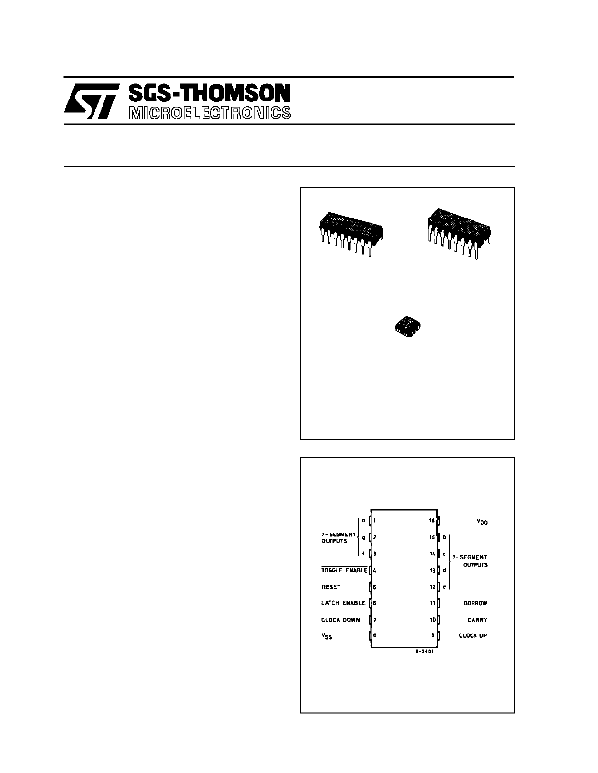
are monolithic integrated circuits, available in 16lead dual in-line plastic or ceramic package. The
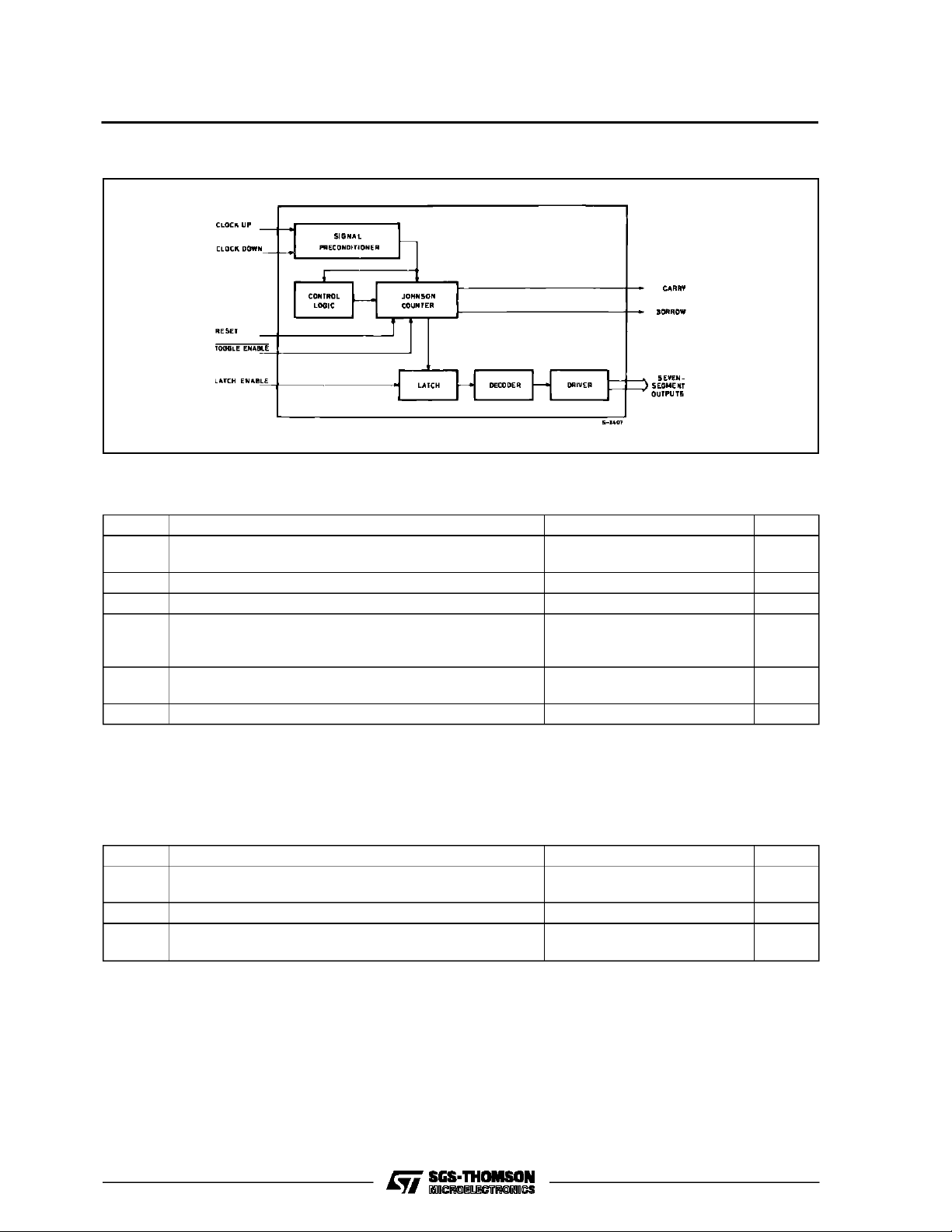
HCC/HCF 40110B is a dual-clocked up/down
counter with a special preconditioning circuit that
allowsthecounter to be clocked, via positive going
inputs, up or down regardless of thatstateor timing
(within100 nstyp.) ofthe other clock line. Theclock
signal is fed into the control logic and Johnson
counter after is preconditioned. The outputs of the
Johnson counter (which include antilock gating to
avoidbeing locked at anillegal state) are fed intoa
latch. This data can be fed directly to the decoder
throughthelatch orcanbestrobedto hold aparticular count whilethe Johnson countercontinuesto be
clocked.The decoder feedsa seven-segment bipolar output driver which can sourceup to 25 mA to
driveLEDs andother displays such as low-voltage
fluorescent and incandescent lamps. A short durationnegative-going pulseappearson theBORROW
output when the count changes from 0 to 9 or the
CARRY output when the count changes from 9 to
0.Atthe other timestheBORROWandCARRYoutput are a logic 1. The CARRY and BORROW outputs can be tied directly to the clock-up and
clock-downlines respectively of another HCC/HCF
40110Bfor easycascading ofseveralcounters.
ORDER CODES :
HCC4 0110BF HCF40110BEY
PIN CONNEC TI O NS
C1
(Chip Carrier)
HCF40110BC1
September 1988
1/11
HCC/HCF40110B
FUN CTIONAL DIAGR A M
ABSOLU TE M AXI MU M R AT ING
Symbol Parameter Value Unit
* Supply Voltage: HCC Types
V
DD
HCF Types
V
P
Input Voltage -0.5 to VDD+ 0.5 V
i
I
DC Input Current (any one input) ± 10 mA
I
Total Power Dissipation (per package)
tot
Dissipation per Output Transistor
for Top = Full Package Temperature Range
T
Operating Temperature: HCC Types
op
HCF Types
T
Stressesabovethoselistedunder ”AbsoluteMaximumRatings”maycausepermanent damagetothedevice. Thisisa stressratingonlyand functional
operation ofthe device atthese oranyotherconditionsabove thoseindicatedintheoperational sections ofthisspecificationisnotimplied.Exposure
to absolute maximumratingconditionsforexternal periodsmay affectdevice reliability.
* All voltagevaluesarereferredto VSSpinvoltage.
Storage Temperature -65 to +150
stg
-0.5 to +20
-0.5 to +18
200
100
-55 to +125
-40 to +85
V
V
mW
mW
o
C
o
C
o
C
RECO MM ENDED OPERAT I N G CO NDITIONS
Symbol Parameter Value Unit
2/11
V
Supply Voltage: HCC Types
DD
HCF Types
V
T
Input Voltage 0 to V
I
Operating Temperature: HCC Types
op
HCF Types
3to18
3to15
DD
-55 to +125
-40 to +85
V
V
V
o
C
o
C
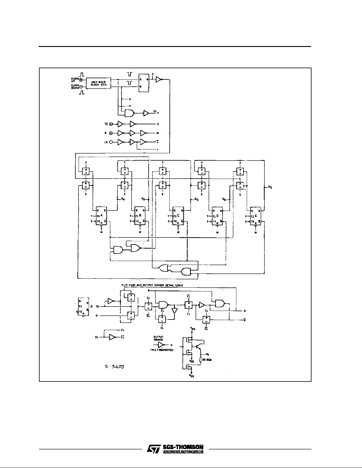
LOGIC DIA GRAMS
HCC/HCF40110
3/11
HCC/HCF40110B
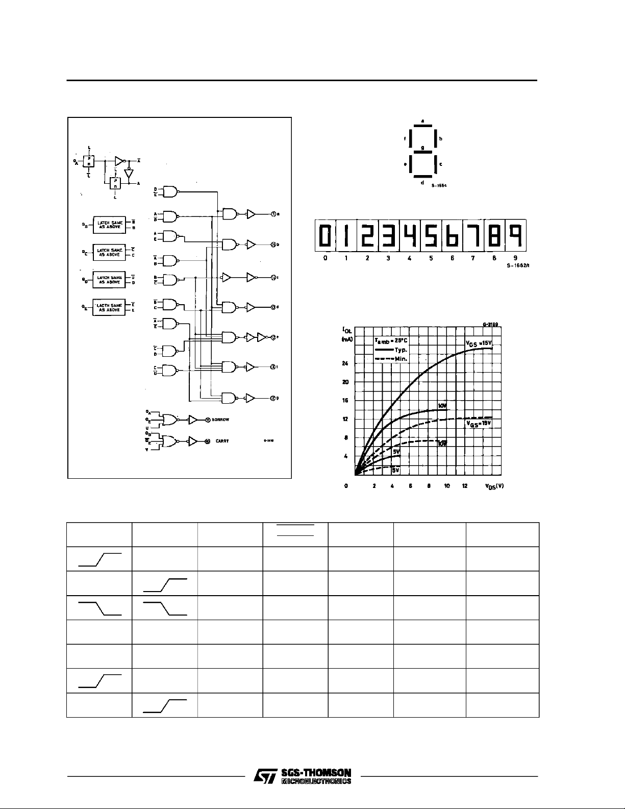
LOGI C DIAGRAM (cont inued) DISPLAY SEGMENTS
Ouptut Low (sink) Current Characterisitcs.
TRUTH TABLE
CLOCK UP*
X 0 0 0 Decrement by 1 Follows Counter
X X X X 1 Goes to 00000
X X X 1 0 Inhibited Remains Fixed
X 1 0 0 Decrement by 1 Remains Fixed
x = Don’tcare 1= High State 2 =LowState
* Typically100 ns between clock-up andclock-down positive transitions are required toensureproper counting
4/11
CLOCK
DOWN*
X 0 0 0 Increments by 1 Follows Counter
X 1 0 0 Increments by 1 Remains Fixed
LATCH
ENABLE
X X 0 No Change No Change
TOGGLE
ENABLE
RESET COUNTER DISPLAY
Follows Counter
(Display = 0 )

HCC/HCF40110
STATI C E LECT RIC AL CHAR ACTER IS TICS (ov e r recommended o peratin g conditions)
Test Conditios Value
Symbol Parameter
Quiescent
I
L
Current
HCC
Types
V
(V)
V
I
(V)
|IO|
(µA)
V
(V)
O
T
DD
*25
LOW
Min. Max. Min. Typ. Max. Min. Max.
0/5 5 5 0.04 5 150
0/10 10 10 0.04 10 300
0/15 15 15 0.04 20 600
o
CT
0/20 20 20 0.48 100 3000
HCF
Types
0/5 5 5 0.04 20 150
0/10 10 10 0.04 40 300
0/15 15 15 0.04 80 600
OH
Output High
V
Voltage
0/5 5 4.95
0/10 10 9.55
0/15 15 14.55
OL
Output Low
V
Voltage
5/0 5 0.05 0 0.05 0.05
10/0 10 0.05 0 0.05 0.05
15/0 15 0.05 0 0.05 0.05
IH
Input High
V
Voltage
0.5/3.8 5 3.5 3.5 3.5
1/8.8 10 7 7 7
1.5/3.8 15 11 11 11
IL
Input Low
V
Voltage
0.5/3.8 5 1.5 1.5 1.5
1/8.8 10 3 3 3
1.5/3.8 15 4 4 4
OL
Output Drive
V
Voltage
(for HCC/HCF)
0 5 4.55
10 5 4.13
25 5 3.64
0 10 9.55
10 10 9.25
25 10 8.85
0 15 14.55
10 15 14.21
25 15 13.9
OL
Output
Sink
Current
HCC
Types
I
HCF
Types
0/5 0.4 5 0.64 0.51 1 0.36
0/10 0.5 10 1.6 1.3 2.6 0.9
0/15 1.5 15 4.2 3.4 6.8 2.4
0/5 0.4 5 0.52 0.44 1 0.36
0/10 0.5 10 1.3 1.1 2.6 0.9
0/15 1.5 15 3.6 3.0 6.8 2.4
I
IH,IIL
C
*T
LOW
*T
HIGH
TheNoiseMargin for both ”1”and”0”levelis:1Vmin.withVDD=5V,2 V min.with VDD=10V,2.5 V min. withVDD=15V
Input
Leakage
Current
Input Capacitance Any Input 5 7.5 pF
I
=-55oCforHCC device:-40oC for HCF device.
=+125oCforHCC device:+85oC for HCF device.
HCC
Types
HCF
Types
0/18
18 ±0.1 ±10
Any Input
0/15 15 ±0.3 ±10
-5
±0.1 ±1
-5
±0.3 ±1
HIGH
Unit
*
µA
V
V
V
V
V
mA
µA
5/11

HCC/HCF40110B
DYNAMIC ELECTRICAL CHARACTERISTICS (T
=25oC, CL=50pF,RL= 200 KΩ,
amb
typic al temperat ure coef f ic ent for all VDDvalues is 03 %/oC, all input rise and fall times = 20 ns)
Symbol Parameter
CLOCK UP/CLOCK DOWN
t
t
t
f
WC
Pulse Width 5 85
W
Maximum Frequency 5 2.5
CL
Carry Pulse Width 5 225
Borrow Pulse Width 5 260
WB
RESET
t
t
PLH
PHL
Propagation Delay Time
Reset to Clock
Delay from Reset to First Allowable Clock 5 300
t
Pulse Width 5 150
W
Test Conditions Value
V
(V) Min. Typ. Max.
DD
10 35
15 15
10 5
15 8
10 100
15 70
10 110
15 80
5 750
10 285
15 200
10 125
15 75
10 60
15 40
Unit
ns
MHz
ns
ns
TEST CIRCUITS
QuiescentDevice Current. Noise Immunity.
6/11

TEST CIRCUITS
Input Leakage Current.
HCC/HCF40110
7/11

HCC/HCF40110B
Plastic DIP16 (0.25) MECHANICAL DATA
DIM.
MIN. TYP. MAX. MIN. TYP. MAX.
a1 0.51 0.020
B 0.77 1.65 0.030 0.065
b 0.5 0.020
b1 0.25 0.010
D 20 0.787
E 8.5 0.335
e 2.54 0.100
e3 17.78 0.700
F 7.1 0.280
I 5.1 0.201
L 3.3 0.130
Z 1.27 0.050
mm inch
8/11
P001C

Ceramic DIP16/1 MECHANICAL DATA
HCC/HCF40110
DIM.
MIN. TYP. MAX. MIN. TYP. MAX.
A 20 0.787
B 7 0.276
D 3.3 0.130
E 0.38 0.015
e3 17.78 0.700
F 2.29 2.79 0.090 0.110
G 0.4 0.55 0.016 0.022
H 1.17 1.52 0.046 0.060
L 0.22 0.31 0.009 0.012
M 0.51 1.27 0.020 0.050
N 10.3 0.406
P 7.8 8.05 0.307 0.317
Q 5.08 0.200
mm inch
P053D
9/11

HCC/HCF40110B
PLCC20 MECHANICAL DATA
DIM.
MIN. TYP. MAX. MIN. TYP. MAX.
A 9.78 10.03 0.385 0.395
B 8.89 9.04 0.350 0.356
D 4.2 4.57 0.165 0.180
d1 2.54 0.100
d2 0.56 0.022
E 7.37 8.38 0.290 0.330
e 1.27 0.050
e3 5.08 0.200
F 0.38 0.015
G 0.101 0.004
M 1.27 0.050
M1 1.14 0.045
mm inch
10/11
P027A

HCC/HCF40110
Information furnishedis believed to be accurate and reliable. However, SGS-THOMSON Microelectronicsassumes no responsability forthe
consequences of useof suchinformation nor forany infringement ofpatents or other rights of third partieswhich may results from its use. No
license is granted byimplicationorotherwiseunderany patentorpatentrights of SGS-THOMSON Microelectronics.Specificationsmentioned
in this publication are subjectto changewithout notice.Thispublication supersedesand replaces allinformation previously supplied.
SGS-THOMSON Microelectronicsproductsarenotauthorizedforuse ascriticalcomponentsinlifesupportdevices orsystemswithoutexpress
written approval of SGS-THOMSON Microelectonics.
1994SGS-THOMSON Microelectronics- All Rights Reserved
Australia -Brazil - France - Germany - Hong Kong - Italy - Japan - Korea - Malaysia - Malta -Morocco - The Netherlands-
Singapore -Spain - Sweden- Switzerland - Taiwan - Thailand- UnitedKingdom - U.S.A
SGS-THOMSON Microelectronics GROUP OFCOMPANIES
11/11
 Loading...