

HCC/HCF4009UB
HCC/HCF4010B
HEX BUFFER/CONVERTERS
4009UB–INVERTING TYPE
4010B–NON INVERTING TYPE
.CMOS TO DTL/TTLHEXCONVERTER
.HIGH-TO-LOWLEVEL LOGIC CONVERSION
.MULTIPLEXER: 1-TO-6 OR 6-TO-1
.HIGH”SINK” AND ”SOURCE” CURRENT CA-
PABILITY
.5V, 10V AND 15V PARAMETRIC RATINGS
.MAXIMUM INPUT CURRENT OF 100 µAAT
18V OVER FULL
.PACKAGE AND TEMPERATURE RANGE;
100nA AT 18V AND 25oC
.100% TESTED FOR QUIESCENT CURRENT
AT 20V
.MEETSALLREQUIREMENTSOFJEDECTEN-
TATIVE STANDARD N. 13A, ” STANDARD
SPECIFICATIONSFOR DESCRIPTION OF B
SERIESCMOS DEVICES ”
DESCRIPTION
The HCC4009UB/4010B (extended temperature
range) and the HCF4009UB/4010B (intermediate
temperature range) are monolithic integrated circuits available in 16-lead dual in line plastic or ceramic packagesand plasticmicropackage.
The HCC/HCF4009UB/4010B are inverting and
non-inverting Hex Buffer/Converters, respectively.
Both devicescan be used asCMOS toTTL or DTL
logic-level converters, as current ”sink” or ”source”
driversor as multiplexer (1to 6).
4049UB and 4050B are prefered replacements for
4009UB and4010B, respectively, in bufferapplica-
tions.
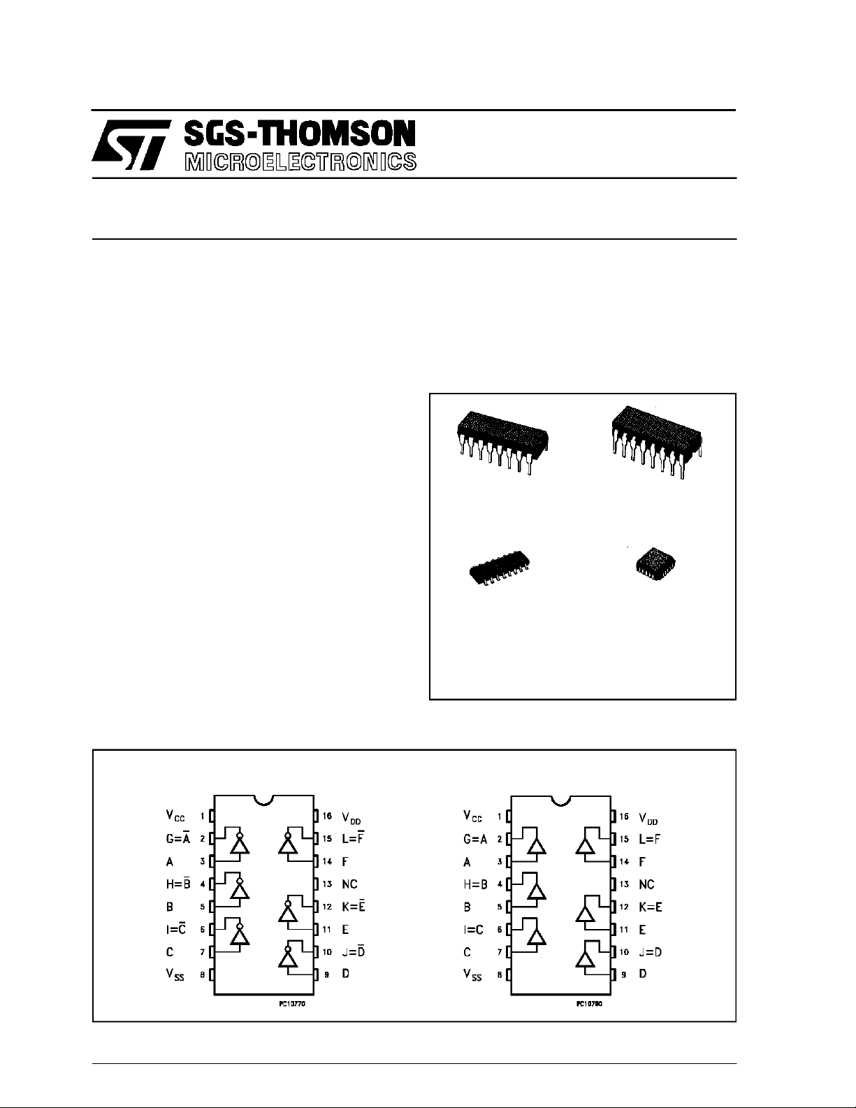
EY
(PlasticPackage)
M1
(MicroPackage)
ORDER CODES :
HCCXXX XBF HCFXXXXBM1
HCFXXXXBEY HCFXXXXBC1
(CeramicPackage)
F
C1
(Chip Carrier)
PIN CONNECTIONS
September 1988
4009UB 4010B
1/13
HCC/HCF4009UB HCC/HCF4010B
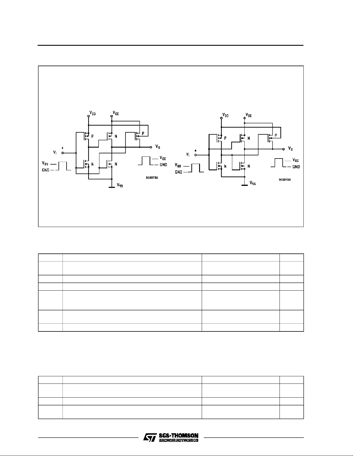
SCHEM ATIC DI A GRA M: C OS/ MOS TO DTL OR TTL CONVERT ER (1 of 6 id entical u ni ts)
4009UB 4010B
ConnectVCCtoDTLorTTLsupply andVDDtoCOS/MOS supply
ABSOLU TE MAXIMU M RATING
Symbol Parameter Value Unit
* Supply Voltage: HCC Types
V
DD
HCF Types
V
P
Input Voltage -0.5 to VDD+ 0.5 V
i
I
DC Input Current (any one input) ± 10 mA
I
Total Power Dissipation (per package)
tot
-0.5 to +20
-0.5 to +18
200
V
V
mW
Dissipation per Output Transistor
for Top = Full Package Temperature Range
T
Operating Temperature: HCC Types
op
HCF Types
T
Stressesabove thoselistedunder ”Absolute Maximum Ratings”maycausepermanent damage tothedevice. Thisisastressratingonlyand functional
operation of the device atthese or anyother conditions above thoseindicated in theoperational sections of thisspecification isnotimplied. Exposure
to absolute maximum ratingconditionsforexternal periods may affectdevice reliability.
* All voltagevalues are referred to VSSpinvoltage.
Storage Temperature -65 to +150
stg
100
-55 to +125
-40 to +85
mW
o
C
o
C
o
C
RECO MM ENDED O PERAT IN G C ONDITIO NS
Symbol Parameter Value Unit
V
Supply Voltage: HCC Types
DD
HCF Types
V
T
Input Voltage 0 to V
I
Operating Temperature: HCC Types
op
HCF Types
3to18
3to15
DD
-55 to +125
-40 to +85
V
V
V
o
C
o
C
2/13
HCC/H CF4009UB HCC/HC F 4010B
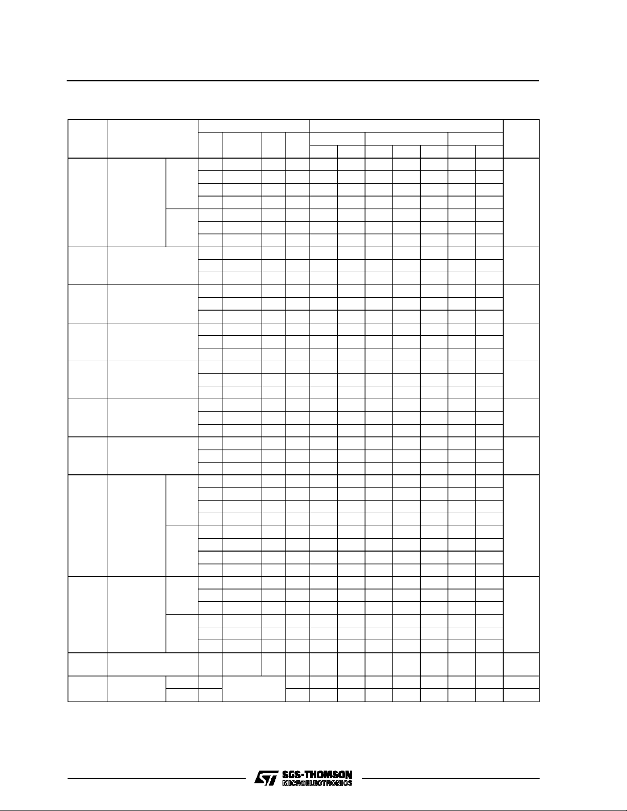
STATI C ELECTRIC AL CHAR ACTER I STI CS (over recomm end ed opera t ing co nditions)
Test Conditios Value
Symbol Parameter
I
Quiescent
L
Current
HCC
Types
V
(V)
V
I
(V)
|IO|
(µA)
V
(V)
O
T
DD
*25
LOW
Min. Max. Min. Typ. Max. Min. Max.
0/5 5 1 0.02 1 30
0/10 10 2 0.02 2 60
0/15 15 4 0.02 4 120
o
CT
0/20 20 20 0.04 20 600
HCF
Types
0/5 5 4 0.02 4 30
0/10 10 8 0.02 8 60
0/15 15 16 0.02 16 120
OH
Output High
V
Voltage
0/5 5 4.95 4.95 4.95
0/10 10 9.95 9.95 9.95
0/15 15 14.95 14.95 14.95
V
OL
Output Low
Voltage
5/0 5 0.05 0.05 0.05
10/0 10 0.05 0.05 0.05
15/0 15 0.05 0.05 0.05
V
Input High
IH
Voltage (4009UB)
0.5 5 4 4 4
11088 8
1.5 15 12.5 12.5 12.5
V
Input High
IH
Voltage (4010B)
4.5 5 3.5 3.5 3.5
91077 7
13.5 15 11 11 11
V
Input Low
IL
Voltage (4009UB)
4.5 5 1 1 1
9102 22
13.5 15 2.5 2.5 2.5
V
Input Low
IL
Voltage (4010B)
0.5 5 1.5 1.5 1.5
1103 33
1.5 15 4 4 4
OH
Output
Drive
Current
HCC
Types
I
0/5 2.5 5 -1 -0.8 -1.6 -0.58
0/5 4.6 5 -0.25 -0.2 -0.4 -0.15
0/10 9.5 10 -0.55 -0.45 -0.9 -0.33
0/15 13.5 15 -1.65 -1.5 -3 -1.1
0/5 2.5 5 -0.9 -0.8 -1.6 -0.65
HCF
Types
0/5 4.6 5 -0.23 -0.2 -0.4 -0.18
0/10 9.5 10 -0.5 -0.45 -0.9 -0.38
0/15 13.5 15 -1.6 -1.5 -3 -1.25
I
OL
Output
Sink
Current
HCC
Types
HCF
Types
0/5 0.4 5 3.75 3 4 2.1
0/10 0.5 10 10 8 10 5.6
0/15 1.5 15 30 24 36 16
0/5 0.4 5 3.6 3 4 2.4
0/10 0.5 10 0.96 8 10 6.4
0/15 1.5 15 40 24 36 1.9
I
IH,IIL
C
*T
LOW
*T
HIGH
TheNoiseMarginfor both ”1” and ”0” level is: 1V min. withVDD=5V,2 V min.withVDD=10V,2.5 V min. withVDD=15V
Input Leakage
Current
Input
I
Capacitance
=-55oCforHCCdevice: -40oC for HCF device.
=+125oCforHCC device:+85oC for HCF device.
4009UB Any Input 15 22.6
4010B 5 7.5 pF
0/18 18 ±0.1 ±10
-5
±0.1 ±1 µA
HIGH
Unit
*
µA
V
V
V
V
V
V
mA
mA
3/13
HCC/HCF4009UB HCC/HCF4010B
DYNAMIC ELECTRICAL CHARACTERISTICS (T
=25oC, CL=50pF,RL= 200 KΩ,
amb
typic al temperat ur e coeffic ent for all VDDvalues is 03 %/oC, all input ris e and fall times= 20 ns)
Symbol Parameter
t
PLH
Propagation Delay Time
(4009UB)
t
PLH
Propagation Delay Time
(4010B)
t
PHL
Propagation Delay Time
(4009UB)
t
PHL
Propagation Delay Time
(4010B)
t
t
TLH
THL
Transition Time 5 5 5 150 350
Transition Time 5 5 5 35 70
Test Conditions Value
(V) VI(V) VCC(V) Min. Typ. Max.
V
DD
5 5 5 70 140
10 10 10 40 80
10 10 5 35 70
15 15 15 30 60
15 15 5 30 60
5 5 5 100 200
10 10 10 50 100
10 10 5 50 100
15 15 15 35 70
15 15 5 35 70
555 3060
10 10 10 20 40
10 10 5 15 30
15 15 15 15 30
15 15 5 10 20
5 5 5 65 130
10 10 10 35 70
10 10 5 30 70
15 15 15 25 50
15 15 5 20 40
10 10 10 75 150
15 15 15 55 110
10 10 10 20 40
15 15 15 15 30
Unit
ns
ns
ns
ns
ns
ns
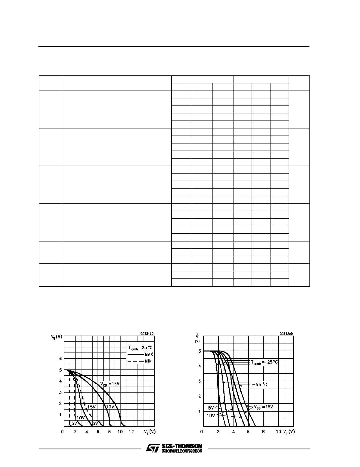
Minimum and Maximum Voltage Transfer Characteristics for 4009UB
4/13
Typical Voltage Transfer Characteristics As a
Function of Temperature for 4009UB

HCC/H CF4009UB HCC/HC F 4010B
Minimum and Maximum Voltage Transfer Characteristics for 4010B
Minimum and Maximum Voltage Transfer Characteristics for 4010B
Minimum and Maximum Voltage Transfer Char-
acteristics for 4010B
Typical Voltage Transfer Characteristics As a
Function ot Temperature for 4010B
Typical Output Los (sink) Current Characteristics
Minimum output Low (sink) Current Charac-
teristics
5/13

HCC/HCF4009UB HCC/HCF4010B
Typical Output High (source) Current Characteristics
Typical Low to High Propagation Delay Time vs
Load Capacitance for 4009UB
Minimum output High (source) Current Charac-
teristics
Typical High to Low Propagation Delay Time vs
Load Capacitance for 4009UB
Typical Low to High Propagation Delay Time vs
Load Capacitance for 4010B
6/13
typical High to Low Propagation Delay Time vs
Load Capacitance for 4010B

HCC/H CF4009UB HCC/HC F 4010B
Typical Low to High Transition Time vs Load Capacitance
Typical Dissipation Characteristics
Typical High to Low Transition Time vs Load Ca-
pacitance
7/13

HCC/HCF4009UB HCC/HCF4010B
TEST CIRCUITS
QuiescentDevice Current. Noise Immunity.
Input Leakage Current.
8/13

HCC/H CF4009UB HCC/HC F 4010B
Plastic DIP16 (0.25) MECHANICAL DATA
DIM.
MIN. TYP. MAX. MIN. TYP. MAX.
a1 0.51 0.020
B 0.77 1.65 0.030 0.065
b 0.5 0.020
b1 0.25 0.010
D 20 0.787
E 8.5 0.335
e 2.54 0.100
e3 17.78 0.700
F 7.1 0.280
I 5.1 0.201
L 3.3 0.130
Z 1.27 0.050
mm inch
P001C
9/13

HCC/HCF4009UB HCC/HCF4010B
Ceramic DIP16/1 MECHANICAL DATA
DIM.
MIN. TYP. MAX. MIN. TYP. MAX.
A 20 0.787
B 7 0.276
D 3.3 0.130
E 0.38 0.015
e3 17.78 0.700
F 2.29 2.79 0.090 0.110
G 0.4 0.55 0.016 0.022
H 1.17 1.52 0.046 0.060
L 0.22 0.31 0.009 0.012
M 0.51 1.27 0.020 0.050
N 10.3 0.406
P 7.8 8.05 0.307 0.317
Q 5.08 0.200
mm inch
10/13
P053D

HCC/H CF4009UB HCC/HC F 4010B
SO16 (Narrow) MECHANICAL DATA
DIM.
MIN. TYP. MAX. MIN. TYP. MAX.
A 1.75 0.068
a1 0.1 0.2 0.004 0.007
a2 1.65 0.064
b 0.35 0.46 0.013 0.018
b1 0.19 0.25 0.007 0.010
C 0.5 0.019
c1 45° (typ.)
D 9.8 10 0.385 0.393
E 5.8 6.2 0.228 0.244
e 1.27 0.050
e3 8.89 0.350
F 3.8 4.0 0.149 0.157
G 4.6 5.3 0.181 0.208
L 0.5 1.27 0.019 0.050
M 0.62 0.024
S8°(max.)
mm inch
P013H
11/13

HCC/HCF4009UB HCC/HCF4010B
PLCC20 MECHANICAL DATA
DIM.
MIN. TYP. MAX. MIN. TYP. MAX.
A 9.78 10.03 0.385 0.395
B 8.89 9.04 0.350 0.356
D 4.2 4.57 0.165 0.180
d1 2.54 0.100
d2 0.56 0.022
E 7.37 8.38 0.290 0.330
e 1.27 0.050
e3 5.08 0.200
F 0.38 0.015
G 0.101 0.004
M 1.27 0.050
M1 1.14 0.045
mm inch
12/13
P027A

HCC/H CF4009UB HCC/HC F 4010B
Information furnished is believed to be accurate and reliable.However, SGS-THOMSON Microelectronics assumes no responsability for the
consequences of use of such information nor for any infringement ofpatents or other rights of third parties which may results from its use. No
license is granted byimplication or otherwise under any patent or patent rights ofSGS-THOMSON Microelectronics. Specificationsmentioned
in this publication are subject to changewithout notice.This publication supersedes andreplaces all information previously supplied.
SGS-THOMSON Microelectronicsproductsarenotauthorizedforuse ascriticalcomponentsinlifesupportdevicesorsystemswithoutexpress
written approval of SGS-THOMSON Microelectonics.
1994 SGS-THOMSON Microelectronics- All RightsReserved
Australia - Brazil - France- Germany - Hong Kong - Italy - Japan - Korea - Malaysia - Malta - Morocco - The Netherlands -
Singapore -Spain - Sweden- Switzerland - Taiwan - Thailand - United Kingdom - U.S.A
SGS-THOMSON Microelectronics GROUP OF COMPANIES
13/13
 Loading...