

HCC/H CF4 01 09B
QUAD LOW-TO-HIGH VOLTAGE LEVEL SHIFTER
.INDEPENDENCE OF POWER SUPPLY SE-
QUENCE CONSIDERATIONS – VCCCAN EXCEED VDD, INPUT SIGNALS CAN EXCEED
BOTHVCCAND V
DD
.UP AND DOWN LEVEL-SHIFTING CAPA-
BILITY
.THREE-STATE OUTPUTS WITH SEPARATE
ENABLECONTROLS
.STANDARDIZED SYMMETRICAL OUTPUT
CHARACTERISTICS
.QUIESCENT CURRENT SPECIFIED AT 20V
FOR HCC DEVICE
.5V, 10V,AND 15VPARAMETRIC RATINGS
.INPUT CURRENTOF100nA AT18VAND25°C
FOR HCC DEVICE
.100% TESTEDFOR QUIESCENTCURRENT
.MEETSALLREQUIREMENTSOFJEDECTEN-
TATIVE STANDARD N°. 13A, ”STANDARD
SPECIFICATIONS FOR DESCRIPTIONOF ”B”
SERIESCMOS DEVICES”
DESCRIPTION
The HCC40109B (extended temperature range)
and HCF40109B (intermediate temperaturerange)
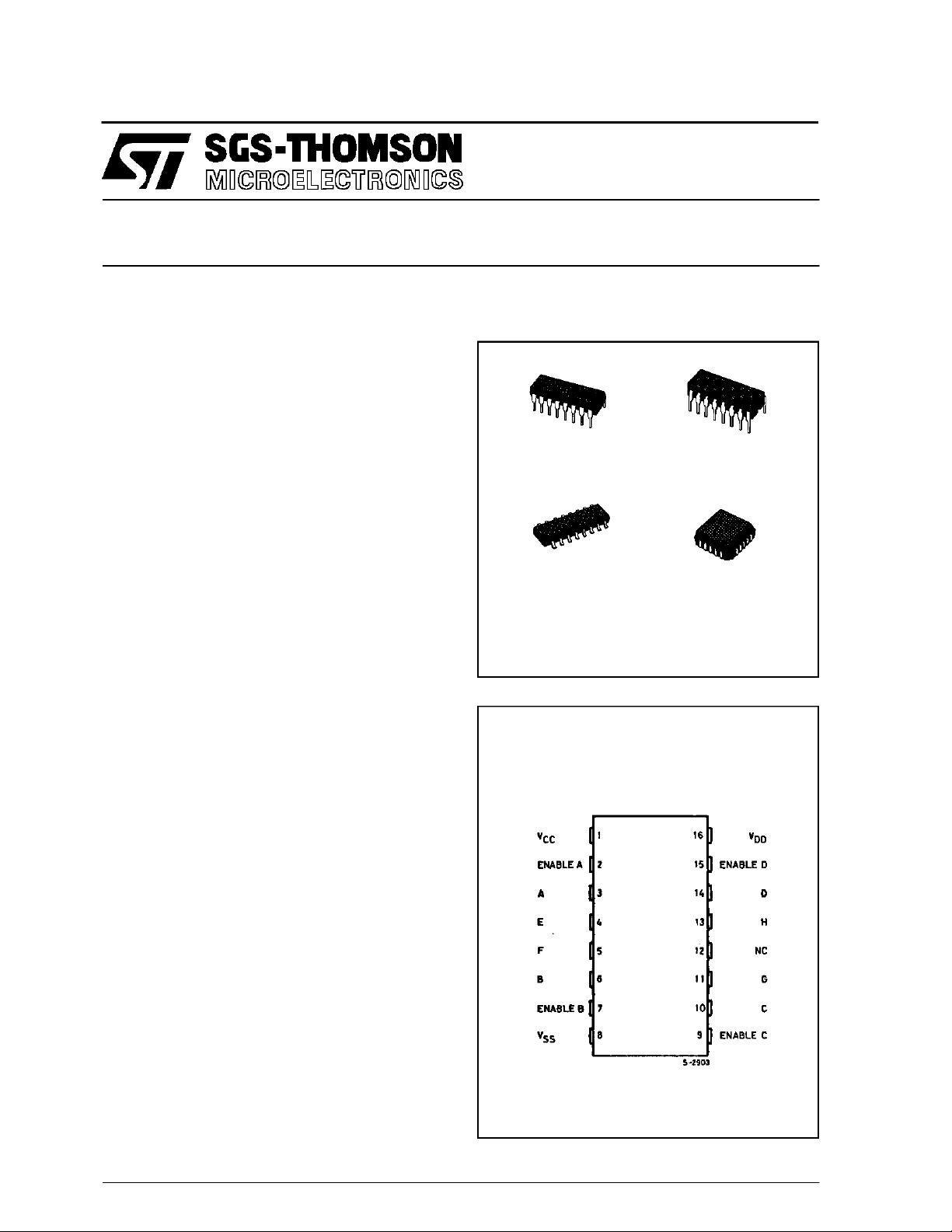
are monolithic integrated circuits, available in 16lead dual in-line plastic or ceramic package and
plastic micropackage. The HCC/HCF40109B con-
tains four low-to-high-voltage level-shifting circuits.
Eachcircuitwill shift a low-voltagedigital-logic input
signal(A, B,C, D) withlogical 1 = VCCand logical 0
=VSStoa higher-voltage output signal(E, F, G, H)
with logical 1 = VDDand logical 0 = VSS. The
HCC/HCF40109B, unlike other low-to-high levelshiftingcircuits, doesnotrequirethepresence ofthe
high-voltage supply (VDD) before the application of
eitherthe low-voltage supply (VCC)or the input signals. There are no restrictions on the sequence of
application of VDD,VCC, or the input signals. In addition, there are no restrictionson the relative magnitudesodthesupplyvoltagesorinput signalswithin
the devicemaximumratings ;VCCmayexceedVDD,
and input signals may exceed VCC, andVDD. When
operated in the mode V
HCC/HCF40109B, will operate as a high-to-low
level-shifter. The HCC/HCF 40109B also features
individual three-state output capability. A low level
on any ofthe separately enabledthree-state output
CC
VDD, the
controls produces a high-impedance state in the
corresponding output.
EY
(Plastic Package)
C1
(Micropackage)
HCC40109BF HCF40109BM1
HCF40109BEY HCF40109BC1
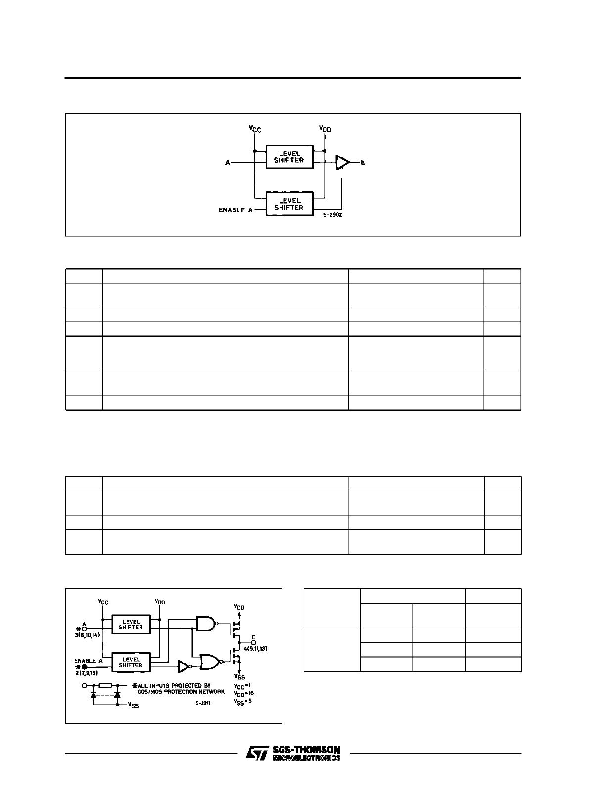
PIN CON NEC TI ONS
(Ceramic Frit SealPackage)
ORDER CODES :
(Plastic ChipCarrier)
F
C1
June 1989
1/12
HCC/HCF40109B
FUNCTIONAL DIAGRAM
1 of4 units
ABSOLUTE MAXI MU M RA TINGS
Symbol Parameter Val ue Unit
* Supply Voltage :HC C Types
V
DD
HCF Types
V
Input Voltage – 0.5 to VDD+ 0.5 V
i
I
DC Input Current (any one input) ± 10 mA
I
P
Total Power Dissipation (per package)
tot
Dissipation per Output Transistor
for T
T
Operating Temperature : HCC Types
op
= Full Package-temperature Range
op
HCF Types
T
Stresses above those listed under ”Absolute Maximum Ratings” may cause permanent damage to the device. This is a stress rating only
and functional operation of the device at these or any other conditions above those indicated in the operational sections of this specification
is not implied. Exposure to absolute maximum rating conditions for external periods may affect device reliability.
* All voltageare with respect to VSS(GND).
Storage Temperature – 65 to + 150 °C
stg
– 0.5to + 20
– 0.5to + 18
200
100
–55to+125
–40to+85
V
V
mW
mW
°C
°C
RECOMMENDED OPERATING CONDITIONS
Symbol Parameter Value Unit
V
T
LOGIC DIAGRAM
2/12
Supply Voltage : HCC Types
DD
HCF Types
V
Input Voltage 0 to V
I
Operating Temperature : HCC Types
op
HCF Types
TRUTH TABLE
Mode
Low to High
Level Shift
LOGIC 0 = LOW (VSS) X = Don’t Care.
LOGIC 1 = VCCat INPUTS and VDDat OUTPUTS.
3to18
3to15
DD
– 55 to + 125
–40to+85
Inputs Outputs
Enable
A, B, C , D
A,B,C,D E,F,G,H
01 0
11 1
X0Z
Z = High Impedance.
V
V
V
°C
°C
HCC/HCF40109B
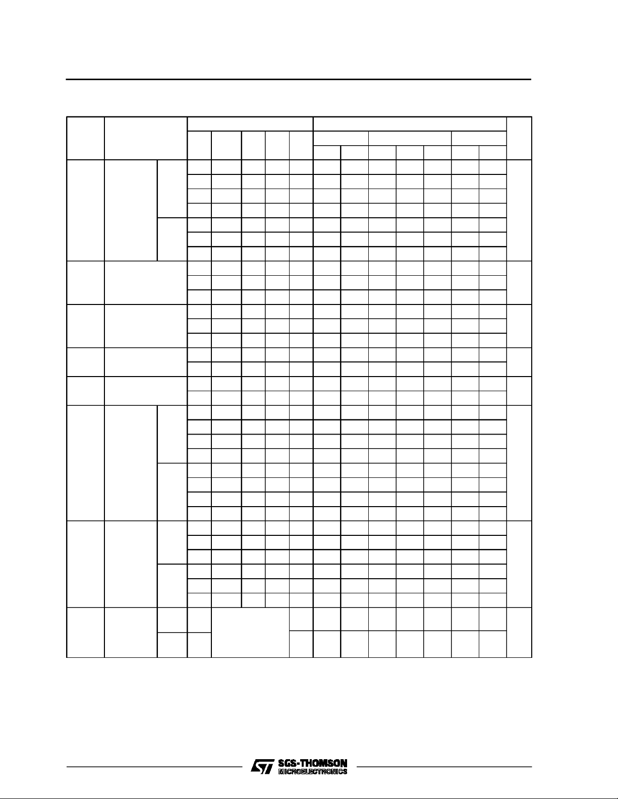
STATIC ELECTRICAL CHARACTERISTICS (over recommended operating conditions)
Test Conditions Value
Symbol Parameter
I
Quiescent
L
Current
HCC
Types
V
V
I
(V)
(V)
0/ 5 5 1 0.02 1 30
0/10 10 2 0.02 2 60
0/15 15 4 0.02 4 120
|
V
|I
O
O
(µA)
(V)
CC
V
(V)
DD
0/20 20 20 0.04 20 600
0/ 5 5 4 0.02 4 30
HCF
Types
0/10 10 8 0.02 8 60
0/15 15 16 0.02 16 120
V
OH
Output High
Voltage
0/ 5 < 1 5 4.95 4.95 4.95
0/10 < 1 10 9.95 9.95 9.95
0/15 < 1 15 14.95 14.95 14.95
V
OL
Output Low
Voltage
5/0 < 1 5 0.05 0.05 0.05
10/0 < 1 10 0.05 0.05 0.05
15/0 < 1 15 0.05 0.05 0.05
V
V
I
Input High Voltage 1/9 < 1 5 10 3.5 3.5 3.5
IH
1.5/13.5
Input Low Voltage 1/9 < 1 5 10 1.5 1.5 1.5
IL
1.5/13.5
OH
Output
Drive
Current
HCC
Types
0/ 5 2.5 5 – 2 – 1.6 – 3.2 – 1.15
0/ 5 4.6 5 – 0.64 – 0.51 – 1 – 0.36
0/10 9.5 10 – 1.6 – 1.3 – 2.6 – 0.9
< 1 10 15 7 7 7
< 1 10 15 3 3 3
0/15 13.5 15 – 4.2 – 3.4 – 6.8 – 2.4
0/ 5 2.5 5 – 1.53 – 1.36 – 3.2 – 1.1
HCF
Types
0/ 5 4.6 5 – 0.52 – 0.44 – 1 – 0.36
0/10 9.5 10 – 1.3 – 1.1 – 2.6 – 0.9
0/15 13.5 15 – 3.6 – 3.0 – 6.8 – 2.4
I
OL
Output
Sink
Current
HCC
Types
0/ 5 0.4 5 0.64 0.51 1 0.36
0/10 0.5 10 1.6 1.3 2.6 0.9
0/15 1.5 15 4.2 3.4 6.8 2.4
0/ 5 0.4 5 0.52 0.44 1 0.36
HCF
Types
0/10 0.5 10 1.3 1.1 2.6 0.9
0/15 1.5 15 3.6 3.0 6.8 2.4
I
IH,IIL
*T
Low
*T
High
TheNoise Margin for both”1” and”0” levelis: 1V min.withVDD=5V, 2V min.with VDD= 10V,2.5V min. withVDD= 15V.
** Forcedoutput disabled.
Input
Leakage
Current
=–55°C for HCC device : – 40°C for HCF device.
= + 125°C for HCC device : + 85°C for HCF device.
HCC
Types
HCF
Types
0/18 18 ± 0.1 ± 10
0/15
15 ± 0.3 ± 10
*25°CT
T
Low
Min Max. Min. Typ. Max. Min. Max.
-5
± 0.1 ± 1
-5
± 0.3 ± 1
High
Unit
*
µA
V
V
V
V
mA
mA
µAAny Input
3/12
HCC/HCF40109B
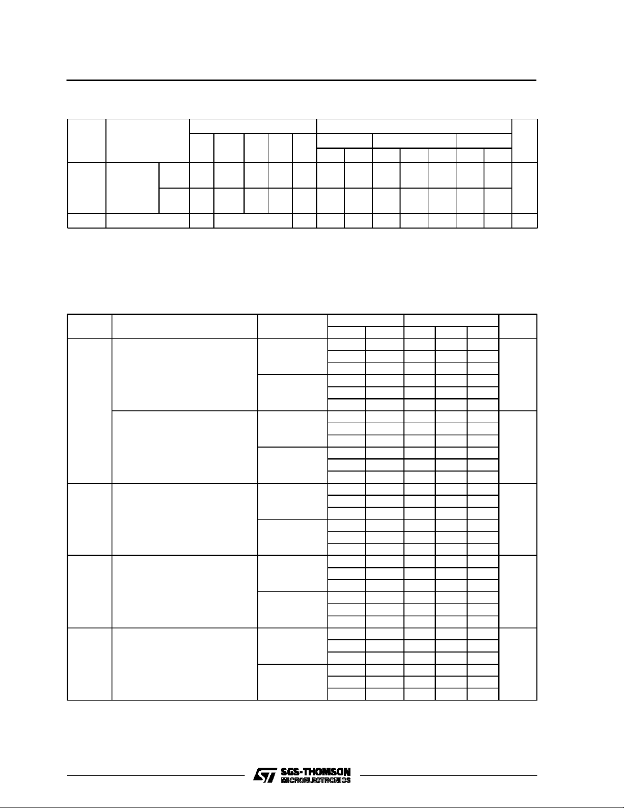
STATIC ELECTRICAL CHARACTERISTICS(continued)
Test Conditions Value
Symbol Parameter
I
,
OH
IOL**
3-State
Output
Leakage
Current
Input Capacitance Any Input 5 7.5 pF
C
I
*T
=–55°C for HCC device : – 40°C for HCF device.
Low
*T
= + 125°C for HCC device : + 85°C for HCF device.
High
TheNoise Margin for both”1” and”0” levelis: 1V min.withVDD=5V, 2V min.with VDD= 10V,2.5V min. withVDD= 15V.
** Forcedoutput disabled.
HCC
Types
HCF
Types
V
V
I
IO VCCV
O
(V) (V) (V) (V) (V)
T
DD
*25°CT
Low
Min. Max. Min. Typ. Max. Min. Max.
0/18 0/18 18 ± 0.4 ±10
0/15 0/15 15 ± 1.0 ±10
-4
± 0.4 ± 12
-4
± 1.0 ± 7.5
High
Unit
*
µA
DYNAMIC ELECTRICAL CHARACTERISTICS(T
=25°C, CL= 50pF, RL= 200kΩ,
amb
typical temperature coefficient for all VDDvalues is 0.3%/°C, all input rise and fall time = 20ns)
Symbol Parameter Shifting Mode
,
t
t
PHL
PLH
Propagation Delay Time
(data input to output)
High to Low Level
L-H
H-L
Low to High Level
L-H
H-L
t
PHZ
3-State Disable Delay Time
Output High to High Impedance
L-H
H-L
t
PZ H
High Impedance to Output High
L-H
H-L
t
PLZ
Output Low to High Impedance
L-H
H-L
Test Conditions Value
V
(V) VDD(V) Min. Typ. Max.
CC
5 10 300 600
5 15 220 440
10 15 180 360
10 5 850 1600
15 5 850 1600
15 10 290 580
5 10 130 260
5 15 120 240
10 15 70 140
10 5 230 460
15 5 230 460
15 10 80 160
5 10 60 120
5 15 50 100
10 15 35 70
10 5 120 240
15 5 120 240
15 10 40 80
5 10 320 640
5 15 230 460
10 15 180 360
10 5 800 1500
15 5 800 1500
15 10 280 560
5 10 370 740
5 15 300 600
10 15 250 500
10 5 850 1600
15 5 850 1600
15 10 350 700
Unit
ns
ns
ns
ns
ns
4/12

HCC/HCF40109B
DYNAMIC ELECTRICAL CHARACTERISTICS(continued)
Symbol Parameter Shifting Mode
t
PZL
High Impedance to Output Low
L-H
H-L
,
t
t
THL
TLH
Transition Time
L-H
H-L
OutputLow (sink)Current Characteristics. Output High(source) Current Characteristics.
Test Conditions Value
V
(V) VDD(V) Min. Typ. Max.
CC
5 10 100 200
5 15 80 160
10 15 40 80
10 5 120 240
15 5 120 240
15 10 40 80
5 10 50 100
515 4080
10 15 40 80
10 5 100 200
15 5 100 200
15 10 50 100
Unit
ns
ns
Typical Transition Timevs. LoadCapacitance. Typical High-to-low Propagation DelayTime vs.
Load Capacitance.
5/12

HCC/HCF40109B
TypicalLow-to-high Propagation Delay Timevs.
Load Capacitance.
High-level Supply Voltage vs. Low-level Supply
Voltage.
TypicalInput Switching vs. High-level SupplyVoltage.
Typical Dynamic Power Dissipation vs. Input Frequency.
TEST CIRCUITS
OutputEnable Delay Times Test Circuit and Waveforms.
6/12

TEST CIRCUITS (continued)
QuiescentDevice Current. Input Voltage.
Input Leakage Current. Dynamic Power Dissipation.
HCC/HCF40109B
7/12
HCC/HCF40109B
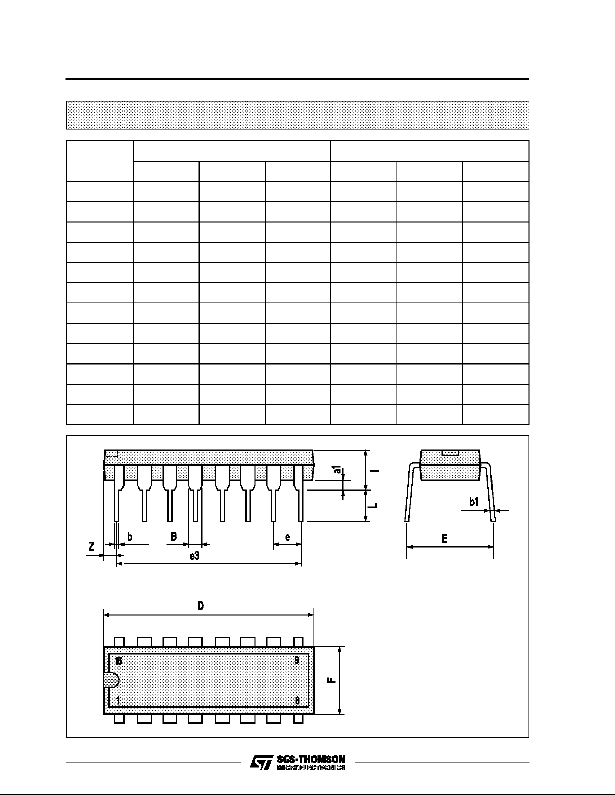
Plastic DIP16 (0.25) MECHANICAL DATA
DIM.
MIN. TYP. MAX. MIN. TYP. MAX.
a1 0.51 0.020
B 0.77 1.65 0.030 0.065
b 0.5 0.020
b1 0.25 0.010
D 20 0.787
E 8.5 0.335
e 2.54 0.100
e3 17.78 0.700
F 7.1 0.280
I 5.1 0.201
L 3.3 0.130
Z 1.27 0.050
mm inch
8/12
P001C

Ceramic DIP16/1 MECHANICAL DATA
HCC/HCF40109B
DIM.
MIN. TYP. MAX. MIN. TYP. MAX.
A 20 0.787
B 7 0.276
D 3.3 0.130
E 0.38 0.015
e3 17.78 0.700
F 2.29 2.79 0.090 0.110
G 0.4 0.55 0.016 0.022
H 1.17 1.52 0.046 0.060
L 0.22 0.31 0.009 0.012
M 0.51 1.27 0.020 0.050
N 10.3 0.406
P 7.8 8.05 0.307 0.317
Q 5.08 0.200
mm inch
P053D
9/12

HCC/HCF40109B
SO16 (Narrow) MECHANICAL DATA
DIM.
MIN. TYP. MAX. MIN. TYP. MAX.
A 1.75 0.068
a1 0.1 0.2 0.004 0.007
a2 1.65 0.064
b 0.35 0.46 0.013 0.018
b1 0.19 0.25 0.007 0.010
C 0.5 0.019
c1 45° (typ.)
D 9.8 10 0.385 0.393
E 5.8 6.2 0.228 0.244
e 1.27 0.050
e3 8.89 0.350
F 3.8 4.0 0.149 0.157
G 4.6 5.3 0.181 0.208
L 0.5 1.27 0.019 0.050
M 0.62 0.024
S8°(max.)
mm inch
10/12
P013H

PLCC20 MECHANICAL DATA
HCC/HCF40109B
DIM.
MIN. TYP. MAX. MIN. TYP. MAX.
A 9.78 10.03 0.385 0.395
B 8.89 9.04 0.350 0.356
D 4.2 4.57 0.165 0.180
d1 2.54 0.100
d2 0.56 0.022
E 7.37 8.38 0.290 0.330
e 1.27 0.050
e3 5.08 0.200
F 0.38 0.015
G 0.101 0.004
M 1.27 0.050
M1 1.14 0.045
mm inch
P027A
11/12

HCC/HCF40109B
Information furnished is believed tobe accurateand reliable.However, SGS-THOMSON Microelectronicsassumes no responsability forthe
consequences of use of such information nor for any infringementof patents or other rights of third partieswhich mayresults from its use.No
license isgranted by implicationor otherwise underany patent or patentrights of SGS-THOMSONMicroelectronics. Specificationsmentioned
in this publication are subject to changewithout notice. This publication supersedes and replaces all information previously supplied.
SGS-THOMSON Microelectronicsproductsare notauthorizedforuse ascritical componentsinlife supportdevices orsystems withoutexpress
written approval of SGS-THOMSON Microelectonics.
1994 SGS-THOMSON Microelectronics - All RightsReserved
Australia - Brazil - France - Germany- HongKong - Italy- Japan - Korea - Malaysia - Malta - Morocco - The Netherlands -
Singapore - Spain - Sweden - Switzerland - Taiwan - Thailand - UnitedKingdom - U.S.A
SGS-THOMSON MicroelectronicsGROUP OF COMPANIES
12/12
 Loading...