

DUAL 2-INPUTNAND BUFFER/DRIVER
.32 TIMES STANDARD B-SERIES OUTPUT
CURRENTDRIVE SINKING CAPABILITY
– 136mATYP. @ VDD= 10V, VDS=1V
.QUIESCENT CURRENT SPECIFIED AT 20V
FOR HCC DEVICE
.5V, 10V, AND 15V PARAMETRIC RATINGS
.INPUT CURRENTOF100nA AT 18V AND25°C
FOR HCC DEVICE
.100% TESTEDFOR QUIESCENTCURRENT
.MEETSALLREQUIREMENTSOFJEDECTEN-
TATIVE STANDARD N°. 13A, ”STANDARD
SPECIFICATIONS FOR DESCRIPTION OF ”B”
SERIESCMOS DEVICES”
HCC/H CF4 01 07B
EY
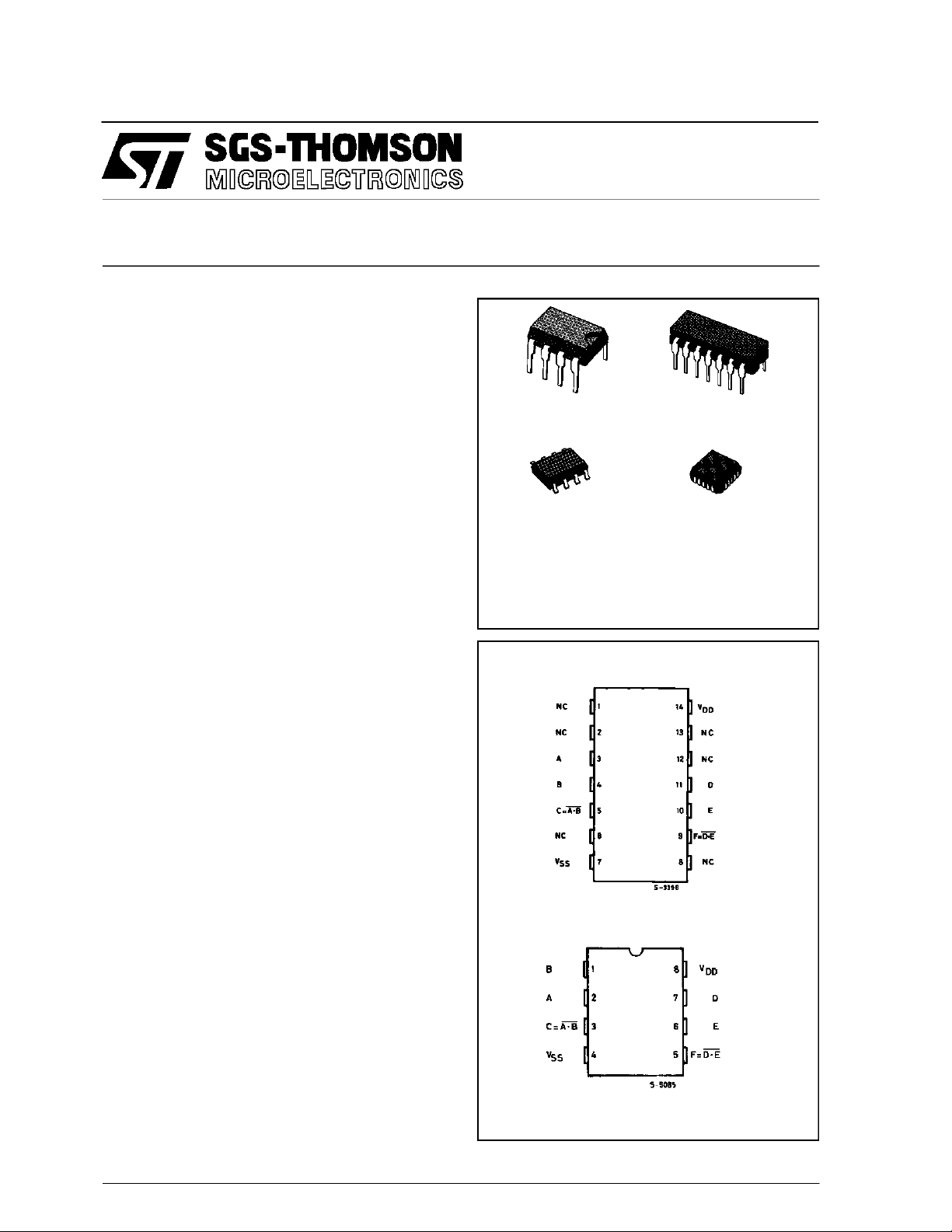
(Plastic Package)F(Ceramic Frit Seal Package)
M1
(MicroPackage)
ORDER CO DES
HCC40107BF HCF40107BM1
HCF40107BEY HCF40107BC1
(Plastic Chip Carrier)
C1
DESCRIPTION
The HCC40107B (extended temperature range)
andHCF40107B (intermediate temperature range)
are monolithic integrated circuits, available in 14lead dual in-line ceramic package 8-lead minidip
plastic package and 8-lead plastic micropackage.
The HCC/HCF40107B is a dual 2-input NANDbuf-
fer/driver containing twoindependent 2-inputNAND
buffers with open-drain single n-channel transistor
outputs. This device features a wired-OR capability
and high output sink current capability (136mA typ.
at VDD=10V, VDS= 1V).
PIN CONNECTIONS
September 1988
1/14
HCC/HCF40107B
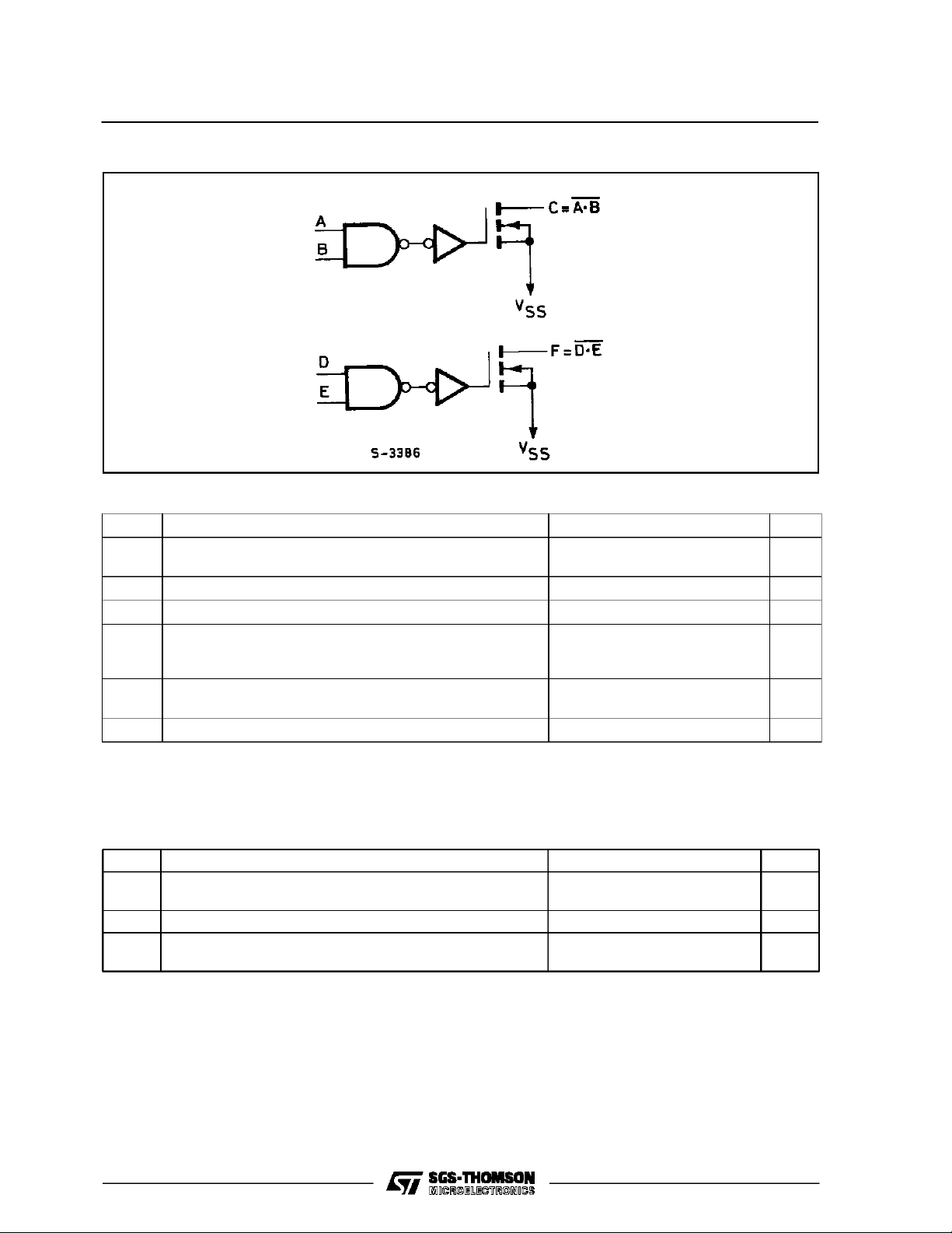
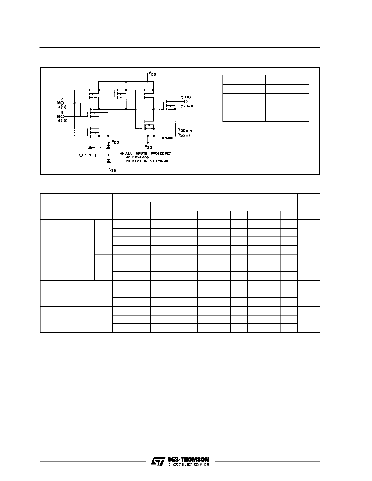
FUN CTIONAL DIAG R A M
ABSOLU TE M AXIMU M R AT INGS
Symbol Parameter Value Unit
V
Supply Voltage : HCC types
*
DD
Input Voltage – 0.5 to VDD + 0.5 V
V
i
DC Input Current (any one input) ± 10 mA
I
I
HCF types
Total Power Dissipation (per package)
P
Dissipation per Output Transistor
tot
for T
= full package-temperature Range
op
Operating Temperature : HCC types
T
op
Storage Temperature – 65 to + 150 °C
T
stg
Stresses above those listed under ”Absolute Maximum Ratings” may cause permanent damage to the device. This is a stress rating only and
functional operation of the device at these or any other conditions above those indicated in the operational sections of this specification is not
implied. Exposure to absolute maximum rating conditions for external periods may affect device reliability.
* All voltages values are referred to VSSpin voltage.
HCF types
– 0.5 to + 20
– 0.5 to + 18
200
100
– 55 to + 125
–40to+85
V
mW
°C
RECOMMENDED OPERATING CONDITIONS
Symbol Parameter Value Unit
V
T
2/14
Supply Voltage : HCC Types
DD
HCF Types
V
Input Voltage 0 to V
I
Operating Temperatu re : HCC Types
op
HCF Types
3to18
3to15
DD
– 55 to + 125
–40to+85
V
V
V
°C
°C
HCC/HCF40107B
SCHEMATIC DIAGRAM AND TRUTH TABLE
AB C
0 0 1* Z
1 0 1* Z
0 1 1* Z
110
* Requires externaland pull-up resis-
)toVDD.
tor (R
L
# Without pull-up resistor(3-state).
STATIC ELECTRICAL CHARACTERISTICS (over recommended operating conditions)
Test Conditions Valu e
Symbol Parameter
Quiescent
I
L
Current
HCC
Types
HCF
Types
V
** Input High
IH
Voltage
V
** Input Low
IL
Voltage
*T
=–55°C for HCC device ; – 40°C for HCF device.
Low
*T
= + 125°C for HCC device ; + 85°C for HCF device.
High
The Noise Margin, full package temperature range, RLto VDD=10kΩ: 1V min withVDD= 5V,2V minwith VDD= 10V, 2.5V min with VDD = 15V.
** Measured with external pull-up resistor, RL= 10kΩ to VDD.
*** Forced output disabled.
V
V
O
|IO|V
I
(V) (V) (µA) (V)
T
DD
* 25°CT
Low
Min. Max. Min. Typ. Max. Min. Max.
High
0/ 5 5 1 0.02 1 30
0/10 10 2 0.02 2 60
0/15 15 4 0.02 4 120
0/20 20 20 0.04 20 600
0/ 5 5 4 0.02 4 30
0/10 10 8 0.02 8 60
0/15 15 16 0.02 16 120
0.5/4.5 < 1 5 3.5 3.5 3.5
1/9 < 1 10 7 7 7
1.5/13.5 < 1 15 11 11 11
4.5 < 1 5 1.5 1.5 1.5
9<110 3 3 3
13.5 < 1 15 4 4 4
#
#
#
Unit
*
µA
V
V
3/14

HCC/HCF40107B
STATIC ELECTRICAL CHARACTERISTICS (continued)
Test Conditions Value
Symbol Parame ter
I
OL
Output
Sink
Current HCC
Types
V
V
O
|IO|V
I
(V) (V) (µA) (V)
T
DD
* 25°CT
Low
Min. Max. Min. Typ. M ax. Min. Max.
High
5 0.4 5 21 16 32 12
51 544 3068 25
10 0.5 10 49 37 74 28
10 1 10 89 68 136 51
15 0.5 15 66 50 100 38
5 0.4 5 17 13.6 32 12
HCF
Types
5 1 5 35.7 25.5 68 22
10 0.5 10 39.1 31.4 74 27
10 1 10 72.2 57.8 136 51
15 0.5 15 53.5 42.5 100 37
I
I
IH,IIL
I
OH,IOL
***
C
*T
*T
The Noise Margin, full package temperature range, RLto VDD=10kΩ: 1V min with VDD= 5V, 2V min withVDD= 10V, 2.5V min withVDD = 15V.
** Measured with external pull-up resistor, RL= 10kΩ to VDD.
*** Forced output disabled.
Output Drive
OH
Current
Input
Leakage
Current
3-State
Output
Leakage
Current
C
Input Capacitance Any Input 5 7.5 pF
I
Output
O
Capacitance
=–55°C for HCC device ; – 40°C for HCF device.
Low
= + 125°C for HCC device ; + 85°C for HCF device.
High
HCC
Types
HCF
Types
HCC
Types
HCF
Types
0/18
Any Input
0/15
0/18 18 18 2 ±10
0/15 15 15 2 ±10
Any Output 30 pF
No Internal Pull-up Device mA
–5
18 ± 0.1 ±10
15 ± 0.3 ±10
± 0.1 ± 1
–5
± 0.3 ± 1
–4
220
–4
220
*
Unit
mA
µA
µA
4/14
HCC/HCF40107B
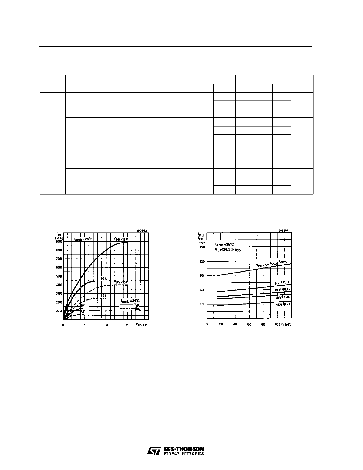
DYNAMIC ELECTRICAL CHARACTERISTICS (T
=25°C, CL= 50pF, typical temperature
amb
coefficient forall VDDvalues is 0.3%/°C, all inputrise and fall time = 20ns)
Symbol Paramet e r
t
,
PHL
t
PL H
Propagation Delay Time
High to Low
Low to High R
t
,
THL
t
TL H
Transition Time
High to Low
Low to High R
*RLis external pull-up resistor to VDD.
Test Conditions
(V) Min. Typ. Max.
V
DD
RL* = 120Ω 5 100 200
10 45 90
15 30 60
* = 120Ω 5 100 200
L
10 60 120
15 50 100
RL* = 120Ω 5 50 100
10 20 40
15 10 20
* = 120Ω 5 50 100
L
10 35 70
15 25 50
Value
Unit
ns
ns
ns
ns
OutputLow (sink) Current Characteristics. TypicalPropagation DelayTime vs. Load Capacit-
ance.
5/14

HCC/HCF40107B
TypicalTransition Time vs. Load Capacitance. TypicalDynamic Power Dissipation vs. Input Fre-
quency.
TYPICAL APPLICATIONS
The bar on the outputline of thislogic diagramindicates that the outputisopen drainas is shown in the previousschematicdiagramand truth table.
LogicDiagram of The HCC/HCF40107B nand
Buffer.
A 2.2-wattIncandescent Lamp-driver Circuit.
Interface of 40107B with Triac,with COS/MOS
Component and Triacisolated.
6/14
Solenoid Driver Circuit.

TYPICAL APPLICATI O NS (contin ued)
Multiplexed Led Circuit.
HCC/HCF40107B
DirectDc DriverInterface of 40107B with a Triac.Line-driver Circuit.
7/14

HCC/HCF40107B
TYPICAL APPLICATI O NS (contin ued)
Motor-controller Circuit.
Led Driver Circuit.
A B Motor Function
O
I
I
O
I
O
O
I
I
I
COUNTER CLOCKWISE
AS PREVIOUS STATE
AS PREVIOUS STATE
OFF
CLOCKWISE
INHIBIT ENABLE OUTPUT
0
1
0
0
TEST CIRCU ITS
Quiescent DeviceCurrent. InputVoltage.
0
0
1
1
OFF
OFF
OFF
ON
8/14

TEST CI RC UIT S (con tinued)
DynamicPowerDissipation.
DynamicPowerDissipation.
HCC/HCF40107B
9/14

HCC/HCF40107B
Minidip (0.4) MECHANICAL DATA
DIM.
MIN. TYP. MAX. MIN. TYP. MAX.
A 3.3 0.130
a1 0.7 0.028
B 1.39 1.65 0.055 0.065
B1 0.91 1.04 0.036 0.041
b 0.5 0.020
b1 0.38 0.5 0.015 0.020
D 9.8 0.386
E 8.8 0.346
e 2.54 0.100
e3 7.62 0.300
e4 7.62 0.300
F 7.1 0.280
I 4.8 0.189
L 3.3 0.130
Z 0.44 1.6 0.017 0.063
mm inch
10/14
P001F

Ceramic DIP14/1 MECHANICAL DATA
HCC/HCF40107B
DIM.
MIN. TYP. MAX. MIN. TYP. MAX.
A 20 0.787
B 7.0 0.276
D 3.3 0.130
E 0.38 0.015
e3 15.24 0.600
F 2.29 2.79 0.090 0.110
G 0.4 0.55 0.016 0.022
H 1.17 1.52 0.046 0.060
L 0.22 0.31 0.009 0.012
M 1.52 2.54 0.060 0.100
N 10.3 0.406
P 7.8 8.05 0.307 0.317
Q 5.08 0.200
mm inch
P053C
11/14

HCC/HCF40107B
SO8 MECHANICAL DATA
DIM.
MIN. TYP. MAX. MIN. TYP. MAX.
A 1.75 0.068
a1 0.1 0.25 0.003 0.009
a2 1.65 0.064
a3 0.65 0.85 0.025 0.033
b 0.35 0.48 0.013 0.018
b1 0.19 0.25 0.007 0.010
C 0.25 0.5 0.010 0.019
c1 45° (typ.)
D 4.8 5.0 0.188 0.196
E 5.8 6.2 0.228 0.244
e 1.27 0.050
e3 3.81 0.150
F 3.8 4.0 0.14 0.157
L 0.4 1.27 0.015 0.050
M 0.6 0.023
S8°(max.)
mm inch
12/14
P013M

PLCC20 MECHANICAL DATA
HCC/HCF40107B
DIM.
MIN. TYP. MAX. MIN. TYP. MAX.
A 9.78 10.03 0.385 0.395
B 8.89 9.04 0.350 0.356
D 4.2 4.57 0.165 0.180
d1 2.54 0.100
d2 0.56 0.022
E 7.37 8.38 0.290 0.330
e 1.27 0.050
e3 5.08 0.200
F 0.38 0.015
G 0.101 0.004
M 1.27 0.050
M1 1.14 0.045
mm inch
P027A
13/14

HCC/HCF40107B
Information furnished is believed to be accurate and reliable.However, SGS-THOMSON Microelectronics assumes no responsability for the
consequences of use of such information nor for any infringement ofpatents or other rights of third parties which may results from its use. No
license isgranted by implicationor otherwise underany patent or patent rights of SGS-THOMSON Microelectronics. Specificationsmentioned
in this publication are subject to changewithout notice. Thispublication supersedes and replaces all information previously supplied.
SGS-THOMSON Microelectronicsproducts are not authorizedforuse ascritical componentsinlife supportdevices orsystems withoutexpress
written approval of SGS-THOMSON Microelectonics.
1994 SGS-THOMSON Microelectronics - All RightsReserved
Australia - Brazil - France - Germany - Hong Kong - Italy - Japan - Korea - Malaysia - Malta - Morocco - The Netherlands -
Singapore - Spain - Sweden - Switzerland - Taiwan - Thailand - United Kingdom - U.S.A
SGS-THOMSON Microelectronics GROUP OF COMPANIES
14/14
 Loading...