

SGS Thomson Microelectronics HCF40103B, HCF40102B, HCC40103B, HCC40102B Datasheet

HCC/HCF40102B
HCC/H CF4 01 03B
8-STAGEPRESETTABLESYNCHRONOUS DOWN COUNTERS
DESCRIPTION
.SYNCHRONOUS OR ASYNCHRONOUS
PRESET
.MEDIUM-SPEED OPERATION : f
CL
= 3.6MHz
(TYP.) @ VDD=10V
.CASCADABLE
.QUIESCENT CURRENT SPECIFIED TO 20V
FOR HCC DEVICE
.5V, 10V AND 15VPARAMETRIC RATINGS
.INPUTCURRENTOF100nAAT18VAND25°C
FOR HCC DEVICE
.100% TESTEDFOR QUIESCENTCURRENT
.MEETSALLREQUIREMENTSOFJEDECTEN-
TATIVE STANDARD No. 13 A, ”STANDARD
SPECIFICATIONS FOR DESCRIPTIONOF ”B”
SERIESCMOS DEVICES”
June 1989
TheHCC40102B, HCC40103B, (extended tempera-
turerange) andthe HCF40102B,HCF40103B (inter-
mediatetemperature range)aremonolithicintegrated
circuits,available in16-lead dual in-line plasticorceramic package. The HCC/HCF40102B,and
HCC/HCF40103Bconsistofan 8-stagesynchronous
downcounterwithasingleoutputwhichisactivewhen
the internal count is zero. The HCC/HCF40102B is
configured astwocascaded 4-bit BCDcounters, and
theHCC/HCF40103B contains a single 8-bit binary
counter. Each typehas controlinputsforenabling or
disabling the clock, for clearing the counter to its
maximum count, and for presetting the counter
eithersynchronously orasynchronously. All control
inputs and the CARRY-OUT/ZERO-DETECT output are active-low logic. In normal operation, the
counter is decremented byone count on eachpositive transition of the CLOCK. Counting is inhibited
when the CARRY-IN/COUNTER ENABLE (CI/CE)
input is high. The CARRY-OUT/ZERO-DETEC
(CO/ZD) output goes low whenthe count reaches
zero if the CI/CE input is low, and remains low for
one full clock period. When the SYNCHRONOUS
PRESET-ENABLE (SPE) input is low, data at the
JAM input is clocked into the counter on the next
positiveclocktransitionregardless ofthestateofthe
CI/CE input. When the ASYNCHRONOUS
PRESET-ENABLE (APE) input is low, data at the
EY
(Plastic Package)
F
(CeramicPackage)
C1
(ChipCarrier)
ORDERCODES :
HCC401XXBF HCF401XXBEY
HCF401XXBC1
PIN CONNEC TI O NS
40102B 2-DECADE BCD TYPE
40103B 8-BIT BINARY TYPE
1/13
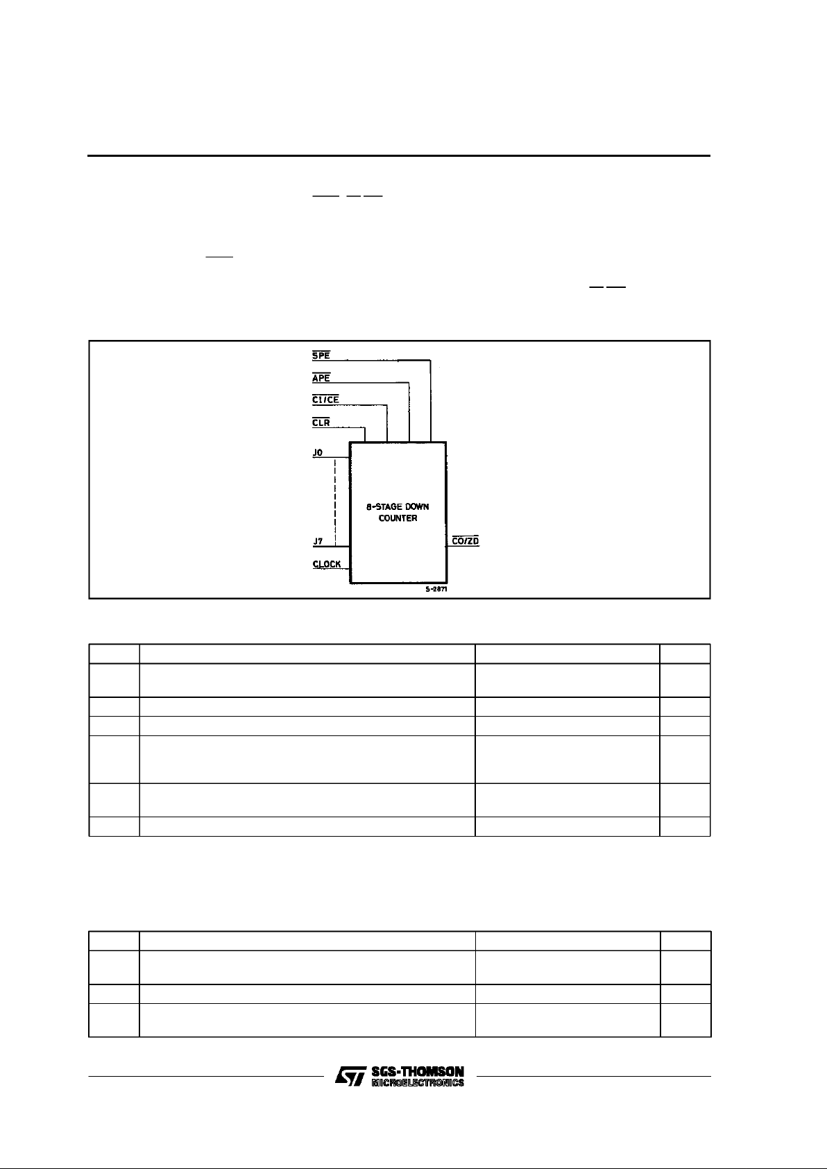
FUNCTIONAL DIAGRAM
ABSOLUTE MAXI MU M RATINGS
Symbol Parame ter Val ue Unit
V
DD
* Supply Voltage :HC C Types
HCF Types
– 0.5to + 20
– 0.5to + 18
V
V
V
i
Input Voltage – 0.5 to VDD+ 0.5 V
I
I
DC Input Current (any one input) ± 10 mA
P
tot
Total Power Dissipation (per package)
Dissipation per Output Transistor
for T
op
= Full Package-temperature Range
200
100
mW
mW
T
op
Operating Temperature : HCC Types
HCF Types
–55to+125
–40to+85
°C
°C
T
stg
Storage Temperature – 65 to + 150 °C
RECOMMENDED OPERATING CONDITIONS
Symbol Parameter Value Unit
V
DD
Supply Voltage : HCC Types
HCF Types
3to18
3to15
V
V
V
I
Input Voltage 0 to V
DD
V
T
op
Operating Temperature : HCC Types
HCF Types
– 55 to + 125
–40to+85
°C
°C
Stresses above those listed under ”Absolute Maximum Ratings” may cause permanent damage to the device. This is a stress rating only
and functional operation of the device at these or any other conditions above those indicated in the operational sections of this specification
is not implied. Exposure to absolute maximum rating conditions for external periods may affect device reliability.
* All voltages are with respect to VSS(GND).
JAM inputs is asynchronously forced into the
counterregardless of the state of the SPE, CI/CE,
or CLOCK inputs. JAM inputsJO-J7 represent two
4-bit BCD words for the HCC/HCF40102B and a
single 8-bit binary word for the HCC/HCF40103B.
When the CLEAR (CLR) input is low, the counter
is asynchronously cleared to its maximum count
(9910for the HCC/HCF40102B and 25510for
theHCC/HCF40103B) regardless of the state of
any other input. The precedence relationship between control input is indicated in thetruth table. If
all control inputs are high atthetiemeofzerocount,
the counterswilljump to themaximum count, giving
a counting sequence of 100 or 256 clock pulses
long.TheHCC/HCF40102B andHCC/HCF40103B
may be cascaded using the CI/CE input and the
HCC/HCF40102B/40103B
2/13

LOGIC DIAGRAMS
40102B
40103B
Detail logic diagram for flip-flops, FF0-FF7used in logic diagrams for 40102B and 40103B.
HCC/HCF40102B/40103B
3/13

LOGIC DIAGRAMS (continued)
40102B
TRUTH TABLE
Control Inputs
CLR APE SPE CI/CE
Preset Mod e Action
1 1 1 1 Inhibit Counter
1 1 1 0 Count Down
110X
Synchronous
Preset on Next Positive Clock Transition
1 0 X X Preset Asynchrounously
0XXX
Asynchronous
Clear to Maximum Count
TimingDiagram for 40102B and 40103B
Notes : 1. 0 = Low level
1 = Highlevel
X = Don’tcare
2. Clock connected toclock input.
3. Synchronous operation : changes occuron negative-to-positive clock transitions..
JAM inputs: HCC/HCF010B ; MSD = J7, J6,J5, J4 (J7 is MSB)
LSD = J3,J2, J1,J0 (J3is MSB)
HCC/HCF40103B Binary ; MSB =J7, LSB =J0
HCC/HCF40102B/40103B
4/13
 Loading...