


DUAL COMPLEMENTARY PAIR PLUS INVERTER
. STANDARDIZED SYMMETRICAL OUTPUT
CHARACTERISTICS
.MEDIUM SPEEDOPERATIONt
(typ.)AT10V
PHL,tPLH
=30ns
.QUIESCENT CURRENT SPECIFIED TO 20V
FOR HCC DEVICE
.INPUT CURRENTOF100nAAT 18VAND25
FOR HCC DEVICE
o
.100% TESTEDFOR QUIESCENTCURRENT
.MEETSALLREQUIREMENTSOFJEDECTEN-
TATIVE STANDARD No13A, ”STANDARD
SPECIFICATIONS FOR DESCRIPTION OF B
SERIESCMOS DEVICES”
HCC4007UB
HCF4007UB
C
EY
(PlasticPackage)
M1
(MicroPackage)
F
(CeramicPackage)
C1
(Chip Carrier)
DESCRIPTION
The HCC4007UBis a monolithic integrated circuit,
available in 14-lead dual in-line plastic or ceramic
package andplastic micropackage.
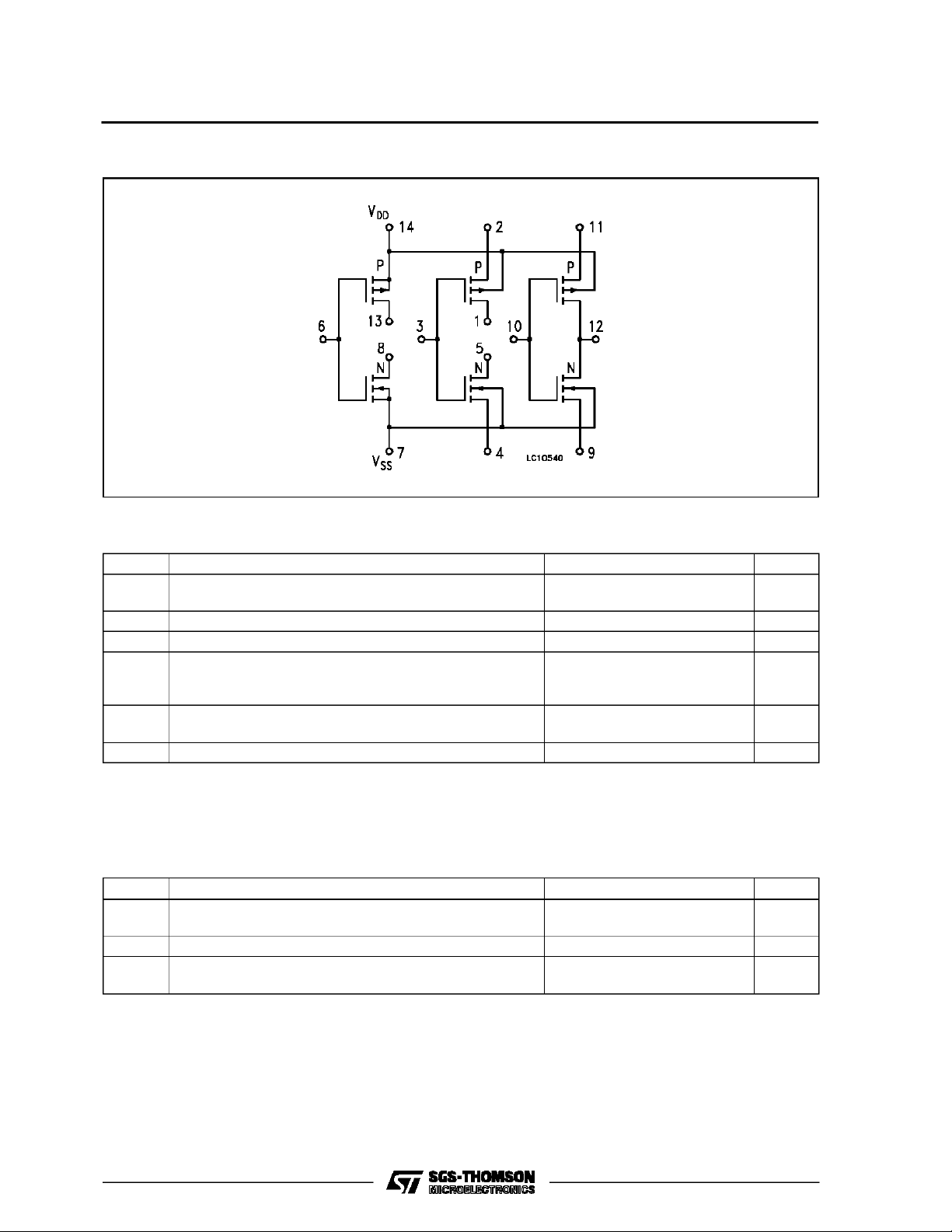
TheHCC4007UB typeis comprised ofthreen-channel and three p-channel enhancement type MOS
transistors. The transistor elements are accessible
throughthepackageterminals toprovide a convenient means for constructing the various typical circuitsasshownintypicalapplications.Morecomplex
functions are possible using multiple packages.
Numbers shown in parentheses indicate terminals
that are connected togetherto formthe varius configurations listed.
HCC4 007UBF HCF4007UBM1
ORDER CODES :
HCF4007UBEY HCF4007UBC1
PIN CONNECTIONS
September 1988
1/14
HCC/HCF4007UB
FUN CTIONAL DIAGR A M
ABSOLU TE M AXIMU M R AT ING
Symbol Parameter Value Unit
V
* Supply Voltage: HCC Types
DD
HCF Types
V
P
Input Voltage -0.5 to VDD+ 0.5 V
i
DC Input Current (any one input) ± 10 mA
I
I
Total Power Dissipation (per package)
tot
-0.5 to +20
-0.5 to +18
200
V
V
mW
Dissipation per Output Transistor
for Top = Full Package Temperature Range
T
Operating Temperature: HCC Types
op
HCF Types
T
Stressesabovethoselistedunder ”Absolute Maximum Ratings”may causepermanent damagetothedevice.This isastressratingonly andfunctional
operation of the device at these or any otherconditions above thoseindicatedintheoperational sections of thisspecification isnotimplied. Exposure
to absolute maximum ratingconditions forexternal periods may affect device reliability.
* All voltagevaluesarereferredto VSSpinvoltage.
Storage Temperature -65 to +150
stg
100
-55 to +125
-40 to +85
mW
o
C
o
C
o
C
RECO MM ENDED OPERATIN G CO NDITIONS
Symbol Parameter Value Unit
V
V
T
Supply Voltage: HCC Types
DD
HCF Types
Input Voltage 0 to V
I
Operating Temperature: HCC Types
op
HCF Types
3to18
3to15
DD
-55 to +125
-40 to +85
V
V
V
o
C
o
C
2/14

SCHEM ATIC DIAGRA M (showing input, output and parasitic diodes)
▲ COS/MOS OUTPUT PROTECTION NETWORK BE-
TWEENTERMINALNOS.1, 2, 4, 5, 8, 9, 11, 12,13, AND
THECORRESPONDINGDRAINSAND/OR SOURCES
❋ COS/MOSINPUT PROTECTIONNETWORK
PARASITICAND NETWORK COMPONENTS
D1 = N+TO P WELL
D2 = P+TO SUBSTRATE
R1 = 1- 5 KΩ
R2=15-30Ω
HCC/HCF4007UB
3/14

HCC/HCF4007UB
STATI C ELE CT RIC AL CHA R ACTE R ISTI CS (ove r reco m mended op er ating condi tions )
Test Conditios Value
Symbol Parameter
Quiescent
I
L
Current
HCC
Types
V
(V)
V
I
(V)
|IO|
(µA)
V
(V)
O
T
DD
*25
LOW
Min. Max. Min. Typ. Max. Min. Max.
0/5 5 0.25 0.01 0.25 7.5
0/10 10 0.5 0.01 0.5 15
0/15 15 1 0.01 1 30
o
CT
0/20 20 5 0.02 5 150
HCF
Types
0/5 5 1 0.01 1 7.5
0/10 10 2 0.01 2 15
0/15 15 4 0.01 4 30
OH
Output High
V
Voltage
0/5 < 1 5 4.95 4.95 4.95
0/10 < 1 10 9.95 9.95 9.95
0/15 < 1 15 14.95 14.95 14.95
OL
Output Low
V
Voltage
5/0 < 1 5 0.05 0.05 0.05
10/0 < 1 10 0.05 0.05 0.05
15/0 < 1 15 0.05 0.05 0.05
IH
Input High
V
Voltage
0.5/4.5 < 1 5 4 4 4
1/9 < 1 10 8 8 8
1.5/13.5 < 1 15 12.5 12.5 12.5
IL
Input Low
V
Voltage
4.5/0.5 < 1 5 1 1 1
9/1 < 1 10 2 2 2
13.5/1.5 < 1 15 2.5 2.5 2.5
OH
Output
Drive
Current
HCC
Types
I
0/5 2.5 5 -2 -1.6 -3.2 -1.15
0/5 4.6 5 -0.64 -0.51 -1 -0.36
0/10 9.5 10 -1.6 -1.3 -2.6 -0.9
0/15 13.5 15 -4.2 -3.4 -6.8 -2.4
0/5 2.5 5 -1.53 -1.36 -3.2 -1.1
HCF
Types
0/5 4.6 5 -0.52 -0.44 -1 -0.36
0/10 9.5 10 -1.3 -1.1 -2.6 -0.9
0/15 13.5 15 -3.6 -3.0 -6.8 -2.4
I
OL
Output
Sink
Current
HCC
Types
HCF
Types
0/5 0.4 5 0.64 0.51 1 0.36
0/10 0.5 10 1.6 1.3 2.6 0.9
0/15 1.5 15 4.2 3.4 6.8 2.4
0/5 0.4 5 0.52 0.44 1 0.36
0/10 0.5 10 1.3 1.1 2.6 0.9
0/15 1.5 15 3.6 3.0 6.8 2.4
I
IH,IIL
Input
Leakage
Current
C
*T
LOW
*T
HIGH
TheNoiseMargin for both ”1” and”0” levelis: 1Vmin.withVDD=5V, 2V min.with VDD=10 V, 2.5 Vmin. withVDD=15V
Input Capacitance Any Input 5 7.5 pF
I
=-55oCforHCC device: -40oC for HCF device.
=+125oCforHCC device: +85oC for HCFdevice.
HCC
Types
HCF
Types
0/18
18 ±0.1 ±10
Any Input
0/15 15 ±0.3 ±10
-5
±0.1 ±1
-5
±0.3 ±1
HIGH
Unit
*
µA
V
V
V
V
mA
mA
µA
4/14

HCC/HCF4007UB
DYNAMIC ELECTRICAL CHARACTERISTICS (T
=25oC, CL=50pF,RL= 200 KΩ,
amb
typic al temperatur e coefficent for all VDDvalues is 03 %/oC, all input ri s e and fall ti mes = 20 ns)
Symbol Parameter
t
t
t
t
PLH
PHL
TLH
THL
Propagation Delay Time 5 55 110
Transition Time 5 100 200
Test Conditions Value
V
(V) Min. Typ. Max.
DD
10 30 60
15 25 50
10 50 100
15 40 80
Unit
ns
ns
Minimum and Maximum Voltage Transfer Characterisctics for Inverterand test Circuit
TypicalCurrent and Voltage Transfer Characteristics for Inverter and Test Circuit
5/14

HCC/HCF4007UB
Typical Voltage Transfer Characteristics for NAND Gate and Test Circuit
Typical Voltage Transfer Characteristics for NOR Gate and Test Circuit
Typical Output Low (Sink) Current Caracteristics Minimum Output Low (Sink) Current Charac-
teristics
6/14

HCC/HCF4007UB
Typical Output High (Source) Current Characteristics
Typical Voltage Transfer Characteristics as a
Function of Temperature
Minimum Output High (Sourrce) Current Characteristics
Typical Propagation Delay Time vs. Load Capacitance
Typical Transition Time vs. Load Capacitance
Typical Dissipatio Per Gate vs. Frequency Characteristics
7/14

HCC/HCF4007UB
TYPICAL APPLICATI O NS (Sam p l e COS/MO S l o gi c circ ui t ar r angements using type 4007U B )
Triple Inverters: (14, 2, 11); (8, 13); (1, 5);
(4, 7, 9).
3-Input NAND Gate: (1, 12, 13); (2, 14, 11);
(4, 8); (5, 9).
3-Input NOR Gate: (13, 2); (1, 11); (12, 5, 8);
(4, 7, 9).
High Sink Current Driver: (6, 3, 10); (8, 5, 12);
(11, 14); (4, 7, 9).
High Source Current Driver: (6, 3, 10);
(13, 1, 12); (14, 2, 11); (7, 9).
8/14
High Sink and Source Current Driver: (6, 3, 10);
(14, 2, 11); (7, 4, 9); (13, 8, 1, 5, 12).

Dual Bidirectional Trasmission Gating: (1, 5, 12); (2, 9); (11, 4); (8, 13, 10); (6, 3).
TEST CIRCUIT
HCC/HCF4007UB
QuiescentDevice Current. Input Voltage.
Input Leakage Current.
9/14

HCC/HCF4007UB
Plastic DIP14 MECHANICAL DATA
DIM.
MIN. TYP. MAX. MIN. TYP. MAX.
a1 0.51 0.020
B 1.39 1.65 0.055 0.065
b 0.5 0.020
b1 0.25 0.010
D 20 0.787
E 8.5 0.335
e 2.54 0.100
e3 15.24 0.600
F 7.1 0.280
I 5.1 0.201
L 3.3 0.130
Z 1.27 2.54 0.050 0.100
mm inch
10/14
P001A

Ceramic DIP14/1 MECHANICAL DATA
HCC/HCF4007UB
DIM.
MIN. TYP. MAX. MIN. TYP. MAX.
A 20 0.787
B 7.0 0.276
D 3.3 0.130
E 0.38 0.015
e3 15.24 0.600
F 2.29 2.79 0.090 0.110
G 0.4 0.55 0.016 0.022
H 1.17 1.52 0.046 0.060
L 0.22 0.31 0.009 0.012
M 1.52 2.54 0.060 0.100
N 10.3 0.406
P 7.8 8.05 0.307 0.317
Q 5.08 0.200
mm inch
P053C
11/14

HCC/HCF4007UB
SO14 MECHANICAL DATA
DIM.
MIN. TYP. MAX. MIN. TYP. MAX.
A 1.75 0.068
a1 0.1 0.2 0.003 0.007
a2 1.65 0.064
b 0.35 0.46 0.013 0.018
b1 0.19 0.25 0.007 0.010
C 0.5 0.019
c1 45° (typ.)
D 8.55 8.75 0.336 0.344
E 5.8 6.2 0.228 0.244
e 1.27 0.050
e3 7.62 0.300
F 3.8 4.0 0.149 0.157
G 4.6 5.3 0.181 0.208
L 0.5 1.27 0.019 0.050
M 0.68 0.026
S8°(max.)
mm inch
12/14
P013G

PLCC20 MECHANICAL DATA
HCC/HCF4007UB
DIM.
MIN. TYP. MAX. MIN. TYP. MAX.
A 9.78 10.03 0.385 0.395
B 8.89 9.04 0.350 0.356
D 4.2 4.57 0.165 0.180
d1 2.54 0.100
d2 0.56 0.022
E 7.37 8.38 0.290 0.330
e 1.27 0.050
e3 5.08 0.200
F 0.38 0.015
G 0.101 0.004
M 1.27 0.050
M1 1.14 0.045
mm inch
P027A
13/14

HCC/HCF4007UB
Information furnishedis believed to be accurate and reliable. However, SGS-THOMSON Microelectronicsassumes no responsability for the
consequences of useof suchinformation nor for any infringement of patents or other rights of third parties which may results from its use. No
license is granted byimplication or otherwiseunder any patentor patentrights ofSGS-THOMSON Microelectronics.Specificationsmentioned
in this publication are subjectto changewithout notice. This publication supersedes andreplaces all information previouslysupplied.
SGS-THOMSON Microelectronicsproducts are not authorized foruse ascritical componentsin life supportdevices or systems without express
written approval of SGS-THOMSON Microelectonics.
1994SGS-THOMSON Microelectronics- All Rights Reserved
Australia -Brazil - France - Germany - Hong Kong - Italy - Japan - Korea - Malaysia - Malta -Morocco - The Netherlands-
Singapore -Spain - Sweden- Switzerland - Taiwan - Thailand- UnitedKingdom - U.S.A
SGS-THOMSON Microelectronics GROUP OFCOMPANIES
14/14
 Loading...