

Page 1
18-STAGESTATIC SHIFT REGISTER
. PERMANENT REGISTER STORAGE WITH
CLOCKLINE ”HIGH”OR ”LOW” ...NO INFORMATION RECIRCULATION REQUIRED
.FULLYSTATIC OPERATION
.SHIFTINGRATES UP TO12MHz @ 10V (typ.)
.STANDARDIZED SYMMETRICAL OUTPUT
CHARACTERISTICS
.QUIESCENT CURRENT SPECIFIED TO 20V
FOR HCC DEVICE
.INPUTCURRENTOF100nA AT18VAND25°C
FOR HCC DEVICE
.100% TESTEDFOR QUIESCENTCURRENT
.5V, 10V, AND 15V PARAMETRIC RATING
.MEETSALLREQUIREMENTSOFJEDECTEN-
TATIVESTANDARDN°13A,”STANDARDSPECIFICATIONS FOR DESCRIPTION OF ”B”
SERIESCMOS DEVICES”
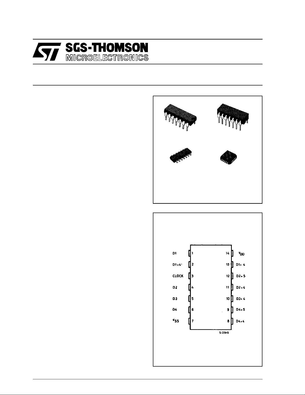
HCC/HCF4006B
EY
(Plastic Package)
M1
(MicroPackage)
ORDERCODES :
HCC4006BF HCF4006BM1
HCF4006BEY HCF4006BC1
(Ceramic FritSeal Package)
F
C1
(Plastic Chip Carrier)
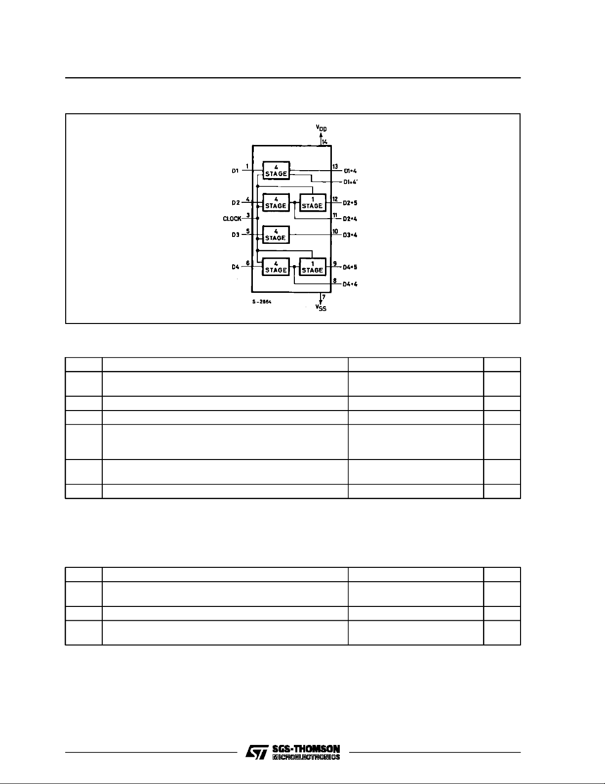
DESC RIPTIO N
TheHCC4006B(extended temperature range) and
the HCF4006B (standard temperature range), are
monolithic integrated circuits, available in 14-lead
dual in-line plastic or ceramic package and plastic
micro package. The types are comprised of 4 separate ”shift register” sections ; two sections of four
stagesand twosections offivestageswithan output
tap at the fourth stage. Each section has an independent”single rail”datapath.Acommonclocksignal is usedfor allstages. Datais shifted to thenext
stage on negative-going transitions of the clock.
Throughappropriate connectionsof inputsandoutputs, multiple register sections of 4, 5, 8, and 9
stages or single register sections of 10, 12, 13, 14,
16, 17 and 18 can be implemented using one
HCC/HCF4006B package. Longer shift register
sectionscanbe assembled byusing more than one
HCC/HCF4006B. To facilitate cascading stages
when clock rise and fall times areslow, an optional
output(D1+4’) that is delayed one-half clock-cycle,
is provided (see truth tablefor output from pin 2).
PIN CONNEC TI O NS
June1989
1/11
Page 2
HCC/HCF4006B
FUNCTIONAL DIAGRAM
ABSOLUTE M AXI MUM RATIN G S
Symbol Parameter Value Unit
V
* Supply Voltage : HCC Types
DD
HCF Types
V
Input Voltage – 0.5 to VDD+ 0.5 V
i
I
DC Input Current (any one input) ± 10 mA
I
P
Total Power Dissipation (per package)
tot
– 0.5 to + 20
– 0.5 to + 18
200
V
V
mW
Dissipation per Output Transistor
for Top= Full Package-temperature Range
T
Operating Temperature : HCC Types
op
HCF Types
T
Stresses above those listed under ”Absolute Maximum Ratings” may cause permanent damage to the device. This is a stress
rating only and functional operation of the device at these or any other conditions above those indicated in the operational sections of this specification is not implied. Exposure to absolute maximum rating conditions for external periods may affect device
reliability.
Storage Temperature – 65 to + 150 °C
stg
100
– 55 to + 125
–40to+85
mW
°C
°C
RECOMMENDED OPERATING CONDITIONS
Symbol Parameter Value Unit
V
T
Supply Voltage : HCC Types
DD
HCF Types
V
Input Voltage 0 to V
I
Operating Temperature : HCC Types
op
HCF Types
3to18
3to15
DD
– 55 to + 125
–40to+85
V
V
V
°C
°C
2/11
Page 3
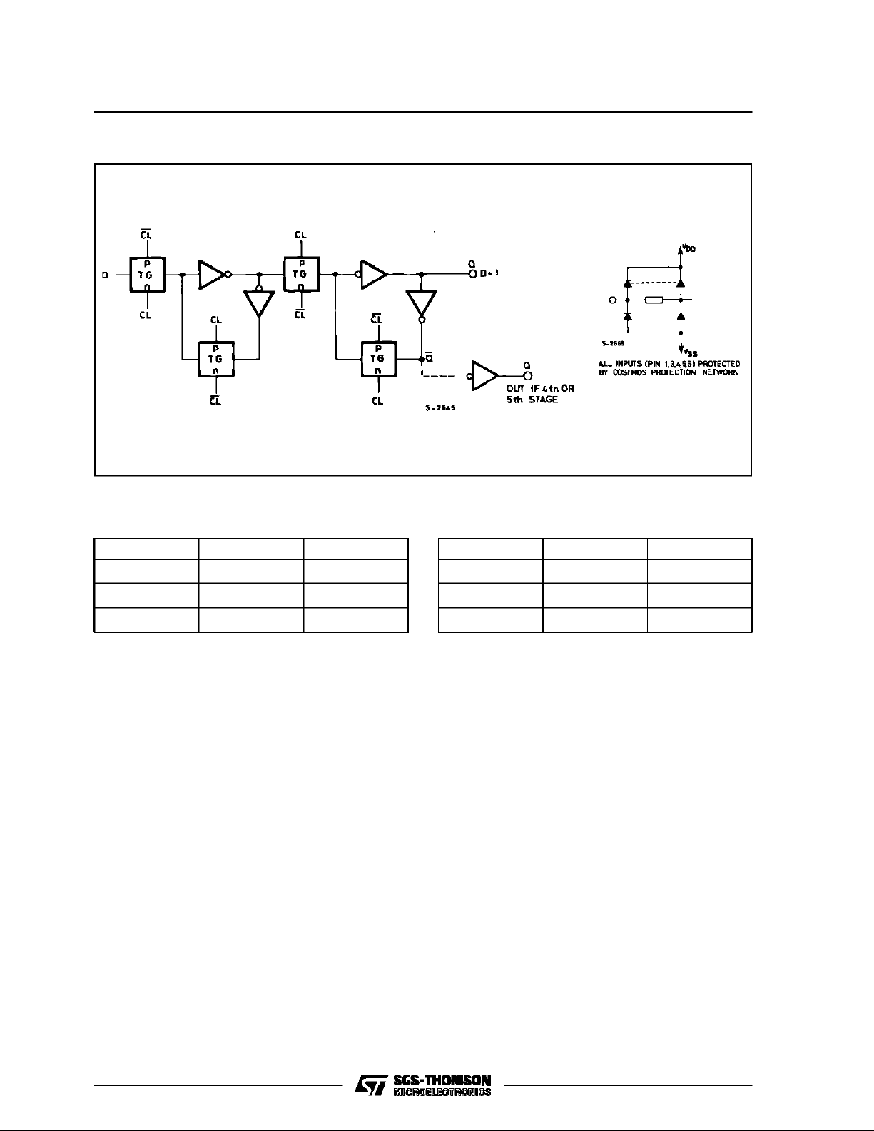
LOGI C DI AG R AM AND TRU TH TABLES ( on e re gister st age)
HCC/HCF4006B
TRUTH TABLE FOR OUTPUT FROM
PIN 2
–
–
–
∆
–
/
–
/
\
–
D1+4’
NC
D1+4 CL
0
1
X
0
1
TRUTH TABLE FOR SHIFT REGISTER
STAGE
DCL
0
1
X
1 = HIGH
0 = LOW
NC = NO CHANGE
∆
–
\
–
–
\
–
–
/
–
X = DON’T CARE
∆ = LEVEL CHANGE
D+1
0
1
NC
3/11
Page 4

HCC/HCF4006B
STATIC ELECTRICAL CHARACTERISTICS (overrecommended operating conditions)
Test Conditions Value
Symbol Parameter
I
Quiescent
L
Current
HCC
Types
HCF
Types
V
OH
Output High
Voltage
V
OL
Output Low
Voltage
V
IH
Input High
Voltage
V
IL
Input Low
Voltage
I
OH
Output
Drive
Current
HCC
Types
HCF
Types
I
Output
OL
Sink
Current
HCC
Types
HCF
Types
I
IH,IIL
Input
Leakage
Current
HCC
Types
HCF
Types
C
Input Capacitance Any Input 5 7.5 pF
I
*T
*T
TheNoise Margin for both”1” and ”0” levelis : 1V min.withVDD=5V, 2V min.withVDD= 10V,2.5 V min.with VDD= 15V.
=–55°CforHCC device : – 40°CforHCF device.
Low
= + 125°CforHCC device : + 85°CforHCF device.
High
V
V
O
|IO|V
I
(V) (V) (µA) (V)
DD
T
* 25° CT
Low
Min. Max. Min. Typ. Max. Min. Max.
0/ 5 5 5 0.04 5 150
0/10 10 10 0.04 10 300
0/15 15 20 0.04 20 600
0/20 20 100 0.08 100 3000
0/ 5 5 20 0.04 20 150
0/10 10 40 0.04 40 300
0/15 15 80 0.04 80 600
0/ 5 < 1 5 4.95 4.95 4.95
0/10 < 1 10 9.95 9.95 9.95
0/15 < 1 15 14.95 14.95 14.95
5/0 < 1 5 0.05 0.05 0.05
10/0 < 1 10 0.05 0.05 0.05
15/0 < 1 15 0.05 0.05 0.05
0.5/4.5 < 1 5 3.5 3.5 3.5
1/9 < 1 10 7 7 7
1.5/13.5 < 1 15 11 11 11
4.5/0.5 < 1 5 1.5 1.5 1.5
9/1 < 1 10 3 3 3
13.5/1.5 < 1 15 4 4 4
0/ 5 2.5 5 – 2 – 1.6 – 3.2 –1.15
0/ 5 4.6 5 – 0. 64 – 0. 51 – 1 – 0.36
0/10 9.5 10 – 1.6 – 1.3 – 2.6 – 0.9
0/15 13.5 15 – 4.2 – 3.4 – 6.8 – 2.4
0/ 5 2.5 5 – 1. 53 – 1. 36 – 3.2 – 1. 1
0/ 5 4.6 5 – 0. 52 – 0. 44 – 1 – 0.36
0/10 9.5 10 – 1.3 – 1.1 – 2.6 – 0.9
0/15 13.5 15 – 3.6 – 3.0 – 6.8 – 2.4
0/ 5 0.4 5 0.64 0.51 1 0.36
0/10 0.5 10 1.6 1.3 2.6 0.9
0/15 1.5 15 4.2 3.4 6.8 2.4
0/ 5 0.4 5 0.52 0.44 1 0.36
0/10 0.5 10 1.3 1.1 2.6 0.9
0/15 1.5 15 3.6 3.0 6.8 2.4
0/18
Any Input
0/15 15 ± 0.3 ±10
18 ± 0.1 ± 10–5± 0. 1 ± 1
–5
± 0. 3 ± 1
High
Unit
*
µA
V
V
V
V
mA
mA
µA
4/11
Page 5
HCC/HCF4006B
DYNAMIC ELECTRICAL CHARACTERISTICS (T
=25°C, CL= 50pF, RL= 200kΩ,
amb
typical temperature coefficient forall VDDvalues is 0.3%/°C, all input rise and fall times = 20ns)
Symbol Parameter
t
PLH,tPHL
Propagation Delay Time 5 200
Test Conditions
V
(V) Min. Typ. Max.
DD
10 100
15 80
t
THL,tTLH
Transition Time 5 100
10 50
15 40
t
Clock Pulse Width 5 100
w
10 45
15 30
t
r,tf
Clock Input Rise or Fall Time* 5 15
10 15
15 15
t
se tu p
Data Setup Time 5 50
10 25
15 20
f
max
Maximum Clock Input Frequency 5 5
10 12
15 16
*
If more than unit is cascaded trCLshould be made less thanor equal to the sum ofthe transition timeand the fixed propagation delay of the
outputof the drivingstagefor the estimatedcapacitive load.
Value
Unit
MHz
ns
ns
ns
µs
ns
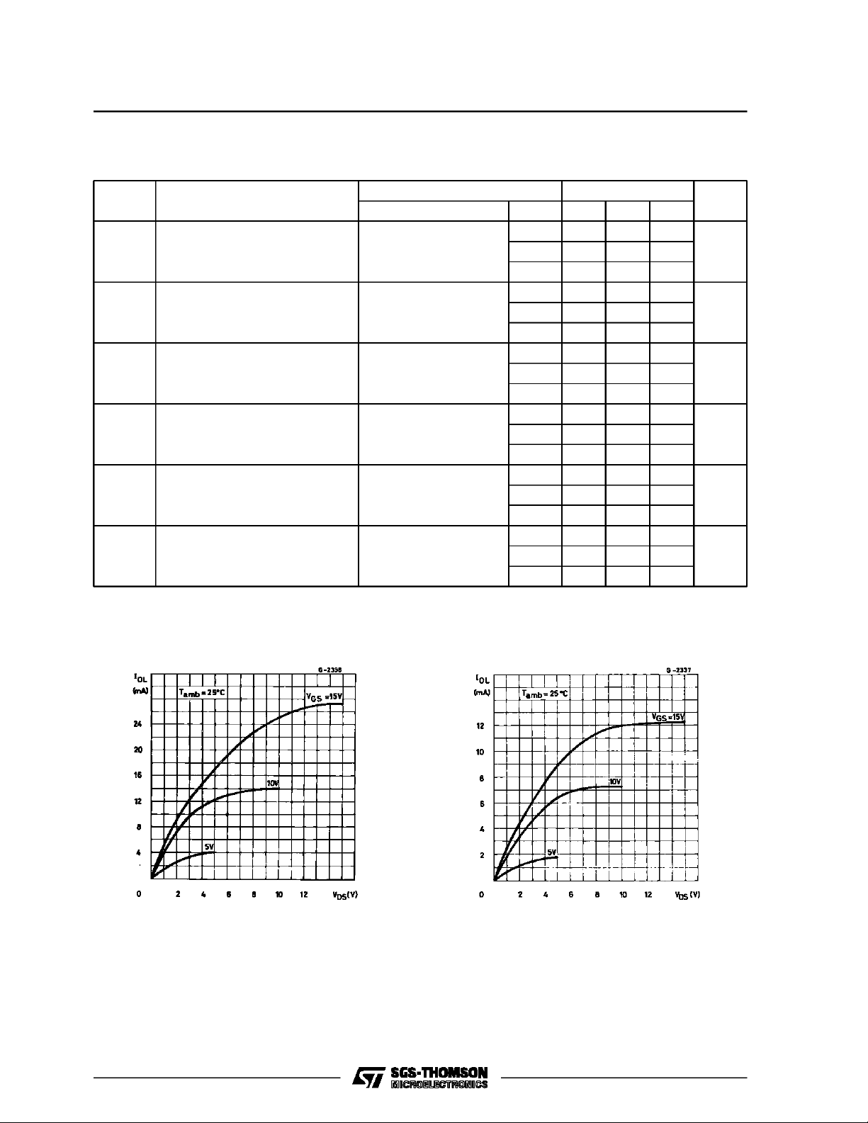
TypicalOutput Low (sink) Current Characteristics.
Minimum Output Low(sink) Current Characteristics.
5/11
Page 6

HCC/HCF4006B
TypicalOutput High (source) Current Characteristics.
TEST CIR CUI TS
QuiescentDevice Current.
Minimum Output High (source)Current Characteristics.
Input Voltage.
Input Current.
6/11
Page 7

Plastic DIP14 MECHANICAL DATA
HCC/HCF4006B
DIM.
MIN. TYP. MAX. MIN. TYP. MAX.
a1 0.51 0.020
B 1.39 1.65 0.055 0.065
b 0.5 0.020
b1 0.25 0.010
D 20 0.787
E 8.5 0.335
e 2.54 0.100
e3 15.24 0.600
F 7.1 0.280
I 5.1 0.201
L 3.3 0.130
Z 1.27 2.54 0.050 0.100
mm inch
P001A
7/11
Page 8

HCC/HCF4006B
Ceramic DIP14/1 MECHANICAL DATA
DIM.
MIN. TYP. MAX. MIN. TYP. MAX.
A 20 0.787
B 7.0 0.276
D 3.3 0.130
E 0.38 0.015
e3 15.24 0.600
F 2.29 2.79 0.090 0.110
G 0.4 0.55 0.016 0.022
H 1.17 1.52 0.046 0.060
L 0.22 0.31 0.009 0.012
M 1.52 2.54 0.060 0.100
N 10.3 0.406
P 7.8 8.05 0.307 0.317
Q 5.08 0.200
mm inch
8/11
P053C
Page 9

SO14 MECHANICAL DATA
HCC/HCF4006B
DIM.
MIN. TYP. MAX. MIN. TYP. MAX.
A 1.75 0.068
a1 0.1 0.2 0.003 0.007
a2 1.65 0.064
b 0.35 0.46 0.013 0.018
b1 0.19 0.25 0.007 0.010
C 0.5 0.019
c1 45° (typ.)
D 8.55 8.75 0.336 0.344
E 5.8 6.2 0.228 0.244
e 1.27 0.050
e3 7.62 0.300
F 3.8 4.0 0.149 0.157
G 4.6 5.3 0.181 0.208
L 0.5 1.27 0.019 0.050
M 0.68 0.026
S8°(max.)
mm inch
P013G
9/11
Page 10

HCC/HCF4006B
PLCC20 MECHANICAL DATA
DIM.
MIN. TYP. MAX. MIN. TYP. MAX.
A 9.78 10.03 0.385 0.395
B 8.89 9.04 0.350 0.356
D 4.2 4.57 0.165 0.180
d1 2.54 0.100
d2 0.56 0.022
E 7.37 8.38 0.290 0.330
e 1.27 0.050
e3 5.08 0.200
F 0.38 0.015
G 0.101 0.004
M 1.27 0.050
M1 1.14 0.045
mm inch
10/11
P027A
Page 11

HCC/HCF4006B
Information furnished is believed to be accurate and reliable. However, SGS-THOMSON Microelectronics assumes no responsability forthe
consequences of useof such information nor forany infringement of patents or other rightsof third parties which may results from its use. No
license isgranted byimplication or otherwise underany patent or patent rights ofSGS-THOMSON Microelectronics. Specificationsmentioned
in this publication are subject to changewithout notice. This publication supersedes andreplaces all information previously supplied.
SGS-THOMSON Microelectronicsproductsare notauthorized for use ascritical componentsinlife supportdevices orsystemswithout express
written approval of SGS-THOMSON Microelectonics.
1994 SGS-THOMSON Microelectronics- All RightsReserved
Australia - Brazil - France - Germany - Hong Kong - Italy - Japan - Korea - Malaysia - Malta - Morocco - The Netherlands -
Singapore - Spain - Sweden- Switzerland- Taiwan - Thailand - United Kingdom - U.S.A
SGS-THOMSON Microelectronics GROUP OF COMPANIES
11/11
 Loading...