

SGS Thomson Microelectronics HCF4077BM1, HCF4077BF, HCF4077BEY, HCF4077BC1, HCF4077B Datasheet
...
4070B–QUAD EXCLUSIVE–OR GATE
4037B–QUAD EXCLUSIVE–NOR GATE
. MEDIUM-SPEED OPERATION t
70ns (typ.) AT VCC= 10V, CL= 50pF
PHL=tPLH
.QUIESCENT CURRENT SPECIFIED TO 20V
FOR HCC DEVICE
.5V, 10V AND 15VPARAMETRIC RATING
.INPUT CURRENT OF 100nA AT 18V AND
25°C FOR HCC DEVICE
.100% TESTEDFOR QUIESCENTCURRENT
.MEETSALLREQUIREMENTSOFJEDECTEN-
TATIVE STANDARD No. 13A, ”STANDARD
SPECIFICATIONS FOR DESCRIPTIONOF ”B”
SERIESCMOS DEVICES”
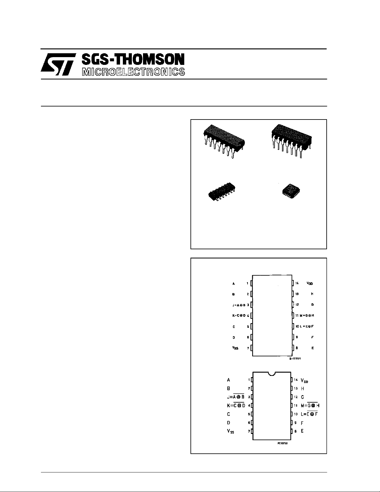
HCC4 07 0/7 7B
HCF4070/77B
GATES
=
EY
(PlasticPackage)
M1
(MicroPackage)
(CeramicPackage)
F
C1
(Chip Carrier)
DESCRIPTION
The HCC4070B/4077B (extended temperature
range) and HCF4070B/4077B (intermediate tem-
perature range) are monolithic integrated circuits,
available in 14-lead dual in-line plastic or ceramic
package and plasticmicropackage.
TheHCC/HCF4070Bcontains fourindependent ex-
clusive-ORgates.
TheHCC/HCF4077Bcontains fourindependent ex-
clusive-NOR gates.
TheHCC/HCF4070B andHCC/HCF4077Bprovide
the system designer with a means for direct implementation of the exclusive-OR and exclusiveNOR function, respectively. For applications as
Logical comparators, Adders/subtractors, Parity generatorsand checkers.
HCC4 0XX BF HCF40XXBM 1
ORDER CODES :
HCF40XXBEY HCF40XXBC1
PIN CONNECTIONS
4070B
4077B
September 1988
1/11

HCC/HCF4070B/4077B
FUN CTIONAL DIAG R A M
4070B 4077B
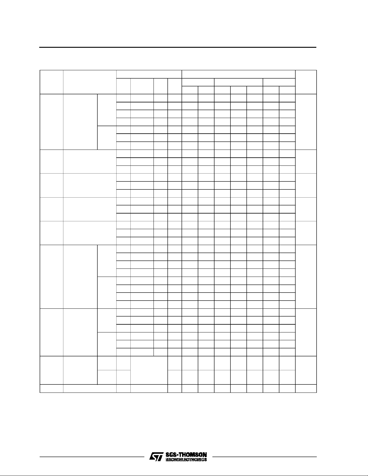
ABSOLU TE MAXIMUM RATING
Symbol Parameter Value Unit
* Supply Voltage: HCC Types
V
DD
HCF Types
V
P
Input Voltage -0.5 to VDD+ 0.5 V
i
I
DC Input Current (any one input) ± 10 mA
I
Total Power Dissipation (per package)
tot
Dissipation per Output Transistor
for Top = Full Package Temperature Range
T
Operating Temperature: HCC Types
op
HCF Types
T
Stressesabove those listedunder”AbsoluteMaximum Ratings”maycausepermanent damagetothedevice.Thisisastressratingonlyand functional
operation of the device at these or any otherconditions above thoseindicated in theoperational sections of thisspecificationisnotimplied.Exposure
to absolute maximum ratingconditionsforexternal periods mayaffect device reliability.
* All voltagevalues are referred to VSSpinvoltage.
Storage Temperature -65 to +150
stg
-0.5 to +20
-0.5 to +18
200
100
-55 to +125
-40 to +85
V
V
mW
mW
o
C
o
C
o
C
RECO MM ENDED OPERAT IN G C ONDITIO NS
Symbol Parameter Value Unit
V
Supply Voltage: HCC Types
DD
HCF Types
V
T
Input Voltage 0 to V
I
Operating Temperature: HCC Types
op
HCF Types
3to18
3to15
DD
-55 to +125
-40 to +85
TRUTH TABLES (1 of 4 gates)
2/11
HCC4070B
ABJ
000
101
011
110
ABJ
001
100
010
111
HCC4077B
V
V
V
o
C
o
C
HCC/HCF4070B/4077B
STATI C ELECTRICAL CHARACTE R ISTI CS (over rec ommended o peratin g conditi ons)
Test Conditios Value
Symbol Parameter
Quiescent
I
L
Current
HCC
Types
V
(V)
V
I
(V)
|IO|
(µA)
V
(V)
O
T
DD
*25
LOW
Min. Max. Min. Typ. Max. Min. Max.
0/5 5 1 0.02 1 30
0/10 10 2 0.02 2 60
0/15 15 4 0.02 4 120
o
CT
0/20 20 20 0.04 20 600
HCF
Types
0/5 5 4 0.02 4 30
0/10 10 8 0.02 8 60
0/15 15 16 0.02 16 120
OH
Output High
V
Voltage
0/5 < 1 5 4.95 4.95 4.95
0/10 < 1 10 9.95 9.95 9.95
0/15 < 1 15 14.95 14.95 14.95
OL
Output Low
V
Voltage
5/0 < 1 5 0.05 0.05 0.05
10/0 < 1 10 0.05 0.05 0.05
15/0 < 1 15 0.05 0.05 0.05
IH
Input High
V
Voltage
0.5/4.5 < 1 5 3.5 3.5 3.5
1/9 < 1 10 7 7 7
1.5/13.5 < 1 15 11 11 11
IL
Input Low
V
Voltage
4.5/0.5 < 1 5 1.5 1.5 1.5
9/1 < 1 10 3 3 3
13.5/1.5 < 1 15 4 4 4
OL
Output
Drive
Current
HCC
Types
I
0/5 2.5 5 -2 -1.6 -3.2 -1.15
0/5 4.6 5 -0.64 -0.51 -1 -0.36
0/10 9.5 10 -1.6 -1.3 -2.6 -0.9
0/15 13.5 15 -4.2 -3.4 -6.8 -2.4
0/5 2.5 5 -1.53 -1.36 -3.2 -1.1
HCF
Types
0/5 4.6 5 -0.52 -0.44 -1 -0.36
0/10 9.5 10 -1.3 -1.1 -2.6 -0.9
0/15 13.5 15 -3.6 -3.0 -6.8 -2.4
I
OL
Output
Sink
Current
HCC
Types
HCF
Types
0/5 0.4 5 0.64 0.51 1 0.36
0/10 0.5 10 1.6 1.3 2.6 0.9
0/15 1.5 15 4.2 3.4 6.8 2.4
0/5 0.4 5 0.52 0.44 1 0.36
0/10 0.5 10 1.3 1.1 2.6 0.9
0/15 1.5 15 3.6 3.0 6.8 2.4
I
IH,IIL
Input
Leakage
Current
C
*T
LOW
*T
HIGH
TheNoiseMarginfor both ”1” and”0”level is: 1V min. withVDD=5V,2 V min.withVDD=10V,2.5 V min. withVDD=15V
Input Capacitance Any Input 5 7.5 pF
I
=-55oCforHCC device:-40oC for HCF device.
=+125oCfor HCCdevice:+85oC for HCF device.
HCC
Types
HCF
Types
0/18
18 ±0.1 ±10
Any Input
0/15 15 ±0.3 ±10
-5
±0.1 ±1
-5
±0.3 ±1
HIGH
Unit
*
µA
V
V
V
V
mA
mA
µA
3/11
HCC/HCF4070B/4077B
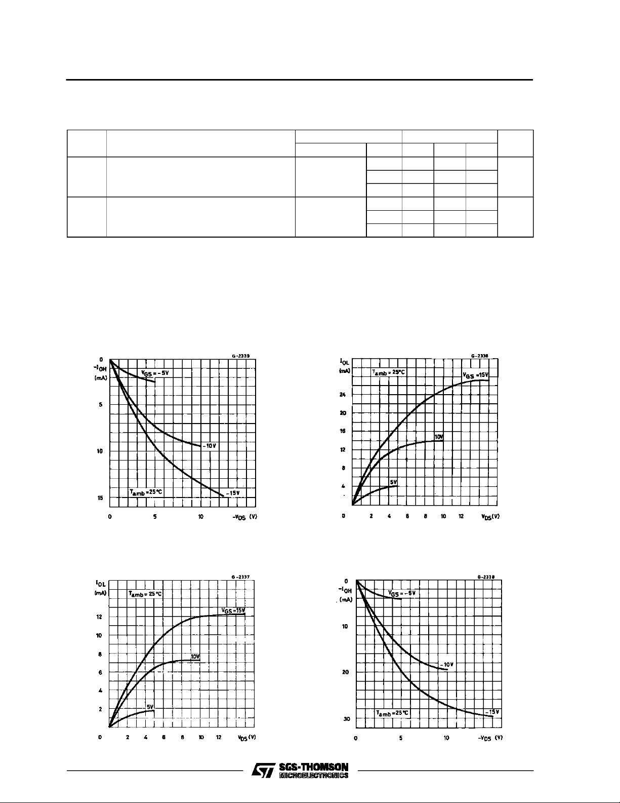
DYNAMIC ELECTRICAL CHARACTERISTICS (T
=25oC, CL=50pF,RL= 200 KΩ,
amb
typic al temperature coeff ic ent for all VDDvalues is 03 %/oC, all input rise and fall ti mes = 20 ns)
Symbol Parameter
t
t
t
t
PLH
PHL
TLH
THL
Propagation Delay Time 5 140 280
Transition Time 5 100 200
Minimum Output High(source) Current Charac-
Test Conditions Value
V
(V) Min. Typ. Max.
DD
10 65 130
15 50 100
10 50 100
15 40 80
TypicalOutput Low (sink)Current.
Unit
ns
ns
teristics.
Minimum Output Low (sink)Current Characteristics.
4/11
TypicalOutput High (source) Current Characteristics.
 Loading...