

Datasheet HCF4017B, HCF4017BM1, HCF4017BF, HCF4017BEY, HCF4017BC1 Datasheet (SGS Thomson Microelectronics)
...
4017B DECADE COUNTER WITH 10
DECOD ED O UTP UT S
4022B OCTAL COUNTER WITH 8
DECOD ED O UTP UT S
.FULLYSTATIC OPERATION
.MEDIUMSPEEDOPERATION-12MHz (typ.)AT
VDD=10V
.STANDARDIZED SYMMETRICAL OUTPUT
CHARACTERISTICS
.QUIESCENT CURRENT SPECIFIED TO 20V
FOR HCC DEVICE
.INPUT CURRENTOF100nA AT18V AND25°C
FOR HCC DEVICE
.100% TESTEDFOR QUIESCENTCURRENT
.5V, 10V, AND 15V PARAMETRIC RATINGS
.MEETSALLREQUIREMENTSOFJEDECTEN-
TATIVE STANDARD N° 13A, ”STANDARD
SPECIFICATIONS FOR DESCRIPTION OF ”B”
SERIESCMOS DEVICES”
HCC/H CF4 01 7B
HCC/HCF4022B
COUNTERS/DIVIDERS
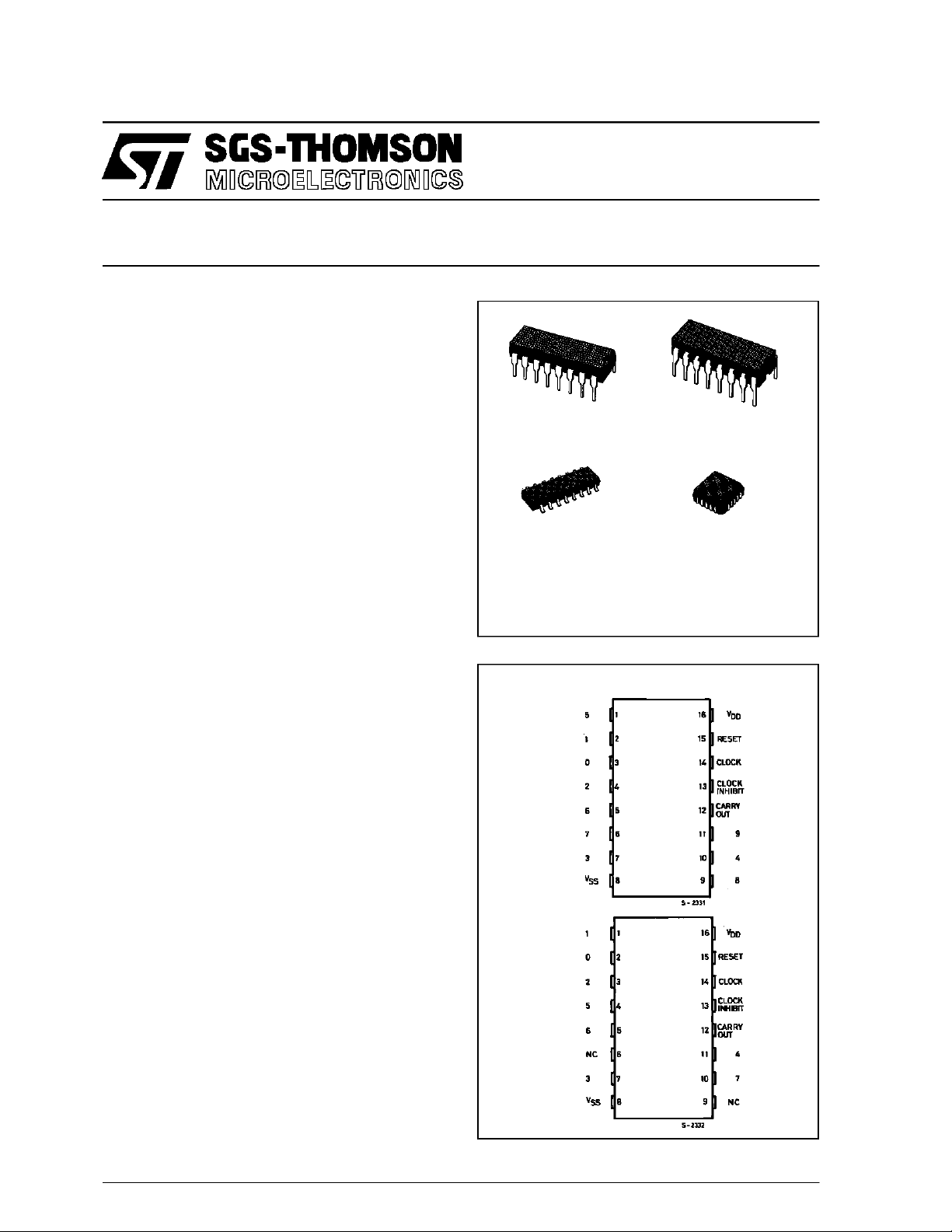
EY
(PlasticPackage)F(Ceramic Frit Seal Package)
M1
(Micro Package)
ORDERCODES :
HCC40XXBF HCF40XXBM1
HCF40XXBEY HCF40XXBC1
(Plastic Chip Carrier)
C1
DESCRIPTIO N
The HCC4017B/4022B (extended temperature
range) and HCF4017B/4022B (intermediate tem-
perature range) are monolithic integrated circuits,
available in 16-lead dual in-line plastic or ceramic
package and plastic micro package.
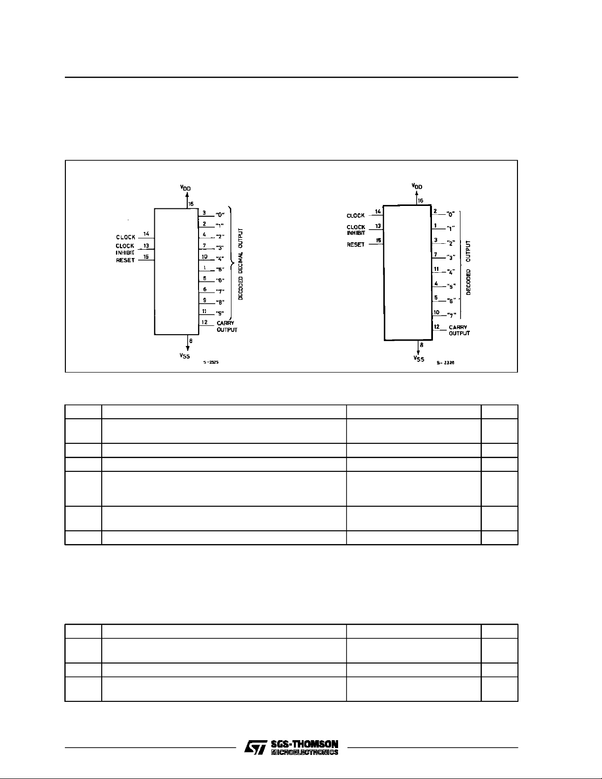
The HCC/HCF4017B and HCC/HCF4022B are 5-
stage and 4-stageJohnson counters having 10and
8 decoded outputs, respectively. Inputs include a
CLOCK, a RESET, and a CLOCK INHIBIT signal.
SchmitttriggeractionintheCLOCKinputcircuit providespulse shapingthatallowsunlimitedclockinput
pulse rise and fall times. These counters are advanced one count at the positive clock signal transition if the CLOCK INHIBIT signal is low. Counter
advancementviathe clocklineisinhibited whenthe
CLOCKINHIBITsignalishigh. AhighRESETsignal
clears the counter to its zero count. Use of the
Johnson decade-counter configuration permits
high-speed operation, 2-input decimal-decode gating, and spike-free decoded outputs. Anti-lock gating is provided, thus assuring proper counting
sequence. The decoded outputs are normally low
and go high only at their respective decoded time
slot. Each decoded output remains high for one full
clock cycle. A CARRY-OUT signal completes one
PIN CONNECTIONS
4017B
4022B
June 1989
1/12
HCC/HCF4017B/4022B
cycle every 10 clock input cycles in the
HCC/HCF4017Borevery8clockinputcyclesin the
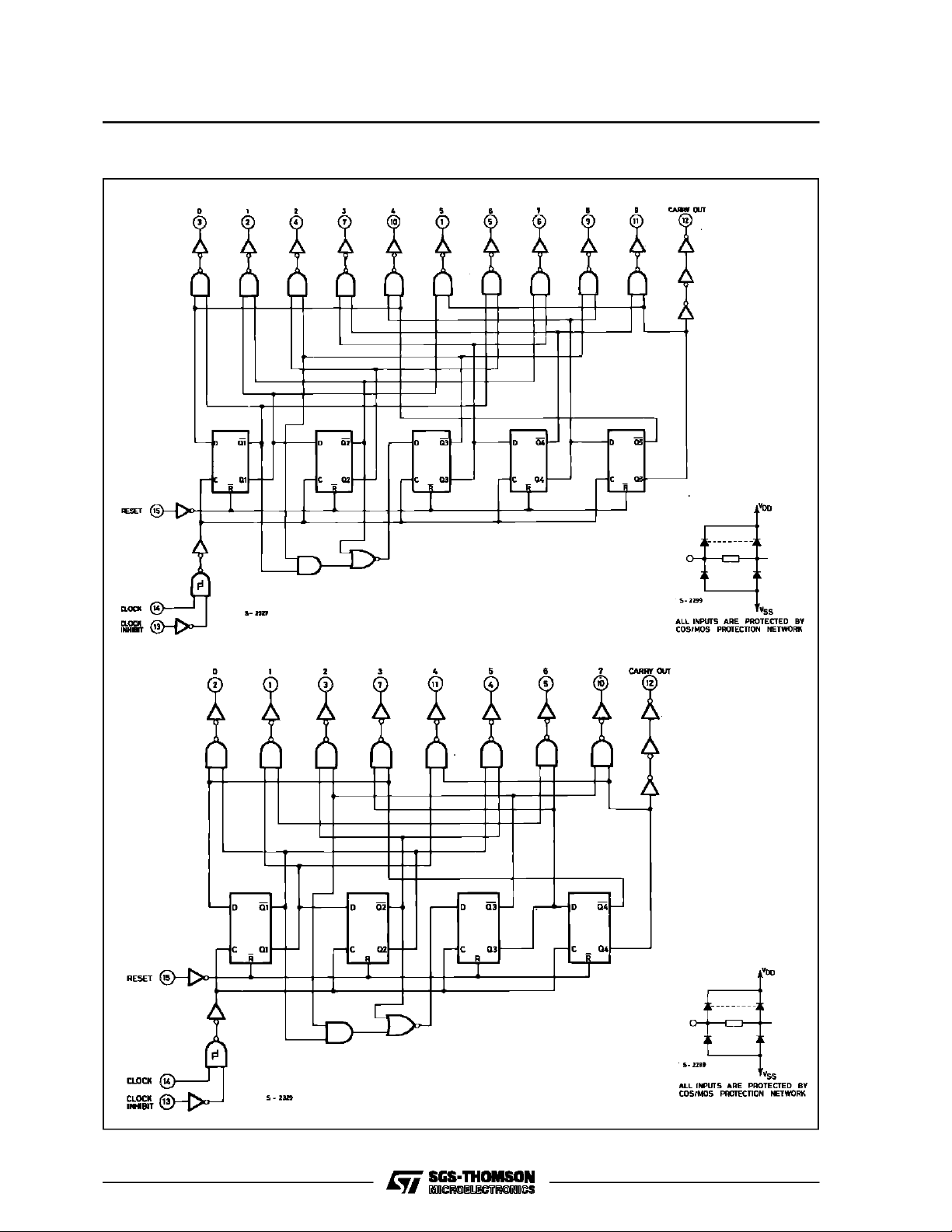
FUN CTIONAL DIAGR A M
4017B
HCC/HCF4022Bandisusedto ripple-clockthesuc-
ceeding device in a multi-device counting chain.
4022B
ABSOLUTE MAXI MUM RAT IN GS
Symbol Parameter Value Unit
V
* Supply Voltage : HCC Types
DD
HCF Types
V
Input Voltage – 0.5 to VDD+ 0.5 V
I
I
DC Input Current (any one input) ± 10 mA
I
P
Total Power Dissipation (per package)
tot
– 0.5 to + 20
– 0.5 to + 18
200
V
V
mW
Dissipation per Output Transistor
for Top= Full Package-temperature Range
T
Operating Temperature : HCC Types
op
HCF Types
T
Stresses above those listed under ”Absolute Maximum Ratings” may cause permanent damage to the device. This is a stress
rating only and functional operation of the device at these or any other conditions above those indicated in the operational sections of this specification is not implied. Exposure to absolute maximum rating conditions for external periods may affect device
reliability.
*
Allvoltagesvaluesare referredto VSSpinvoltage.
Storage Temperature – 65 to + 150 °C
stg
100
– 55 to + 125
–40to+85
mW
°C
°C
RECOMMENDED OPERATING CONDITIONS
Symbol Parameter Value Unit
V
T
Supply Voltage : HCC Types
DD
HCF Types
V
Input Voltage 0 to V
I
Operating Temperature : HCC Types
op
HCF Types
3to18
3to15
DD
– 55 to + 125
–40to+85
V
V
V
°C
°C
2/12
LOGIC DIA GRAMS
4017B
HCC/HCF4017B/4022B
4022
3/12
HCC/HCF4017B/4022B
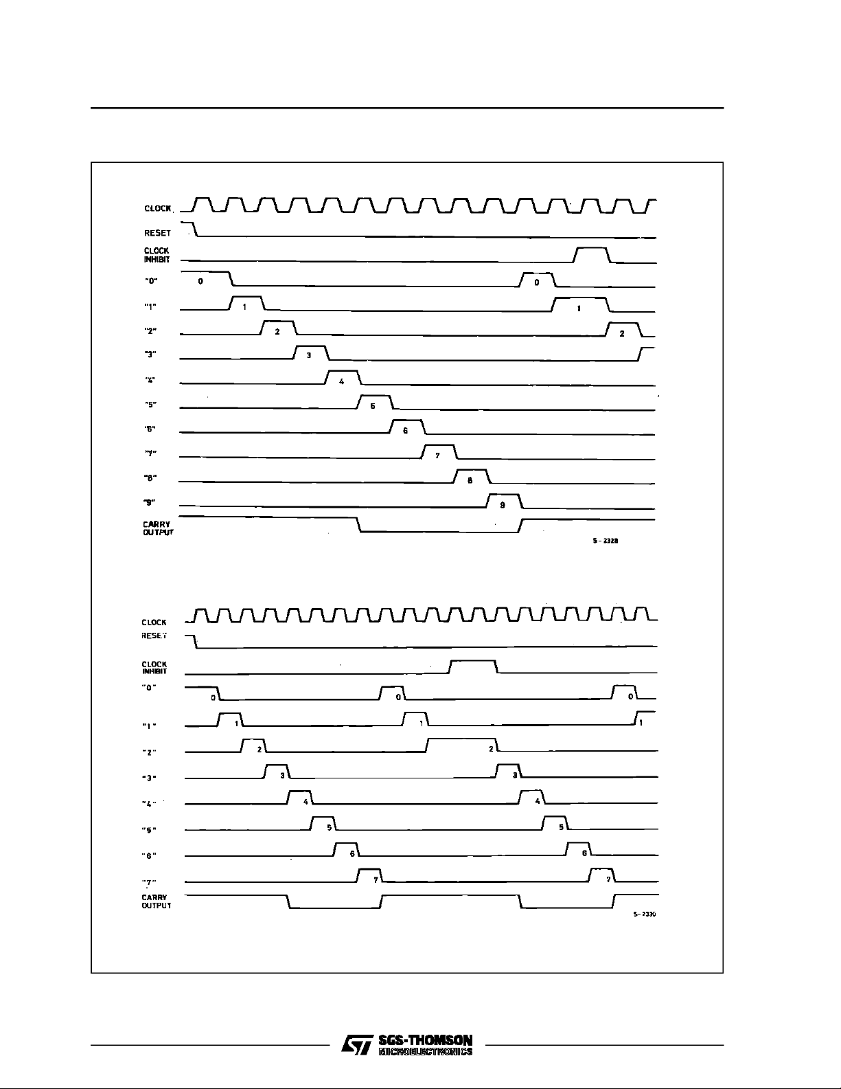
TIM ING D I AG R AMS
4017B
4022B
4/12

HCC/HCF4017B/4022B
STATIC ELECTRICAL CHARACTERISTICS (over recommended operatingconditions)
Test Conditions Value
Symbol Parameter
I
Quiescent
L
Current
HCC
Types
V
V
I
(V) (V) (µA) (V)
|IO|VDDT
O
* 25°CT
Low
High
Min. Max. Min. Typ. Max. Min. Max.
0/ 5 5 5 0.04 5 150
0/10 10 10 0.04 10 300
0/15 15 20 0.04 20 600
0/20 20 100 0.08 100 3000
0/ 5 5 20 0.04 20 150
HCF
0/10 10 40 0.04 40 300
Types
0/15 15 80 0.04 80 600
V
OH
Output High
Voltage
0/ 5 < 1 5 4.95 4.95 4.95
0/10 < 1 10 9.95 9.95 9.95
0/15 < 1 15 14.95 14.95 14.95
V
OL
Output Low
Voltage
5/0 < 1 5 0.05 0.05 0.05
10/0 < 1 10 0.05 0.05 0.05
15/0 < 1 15 0.05 0.05 0.05
V
IH
Input High
Voltage
0.5/4.5 < 1 5 3.5 3.5 3.5
1/9 < 1 10 7 7 7
1.5/13.5 < 1 15 11 11 11
V
IL
Input Low
Voltage
4.5/0.5 < 1 5 1.5 1.5 1.5
9/1 < 1 10 3 3 3
13.5/1.5 < 1 15 4 4 4
I
Output
OH
Drive
Current
0/ 5 2.5 5 – 2 – 1.6 – 3.2 –
HCC
0/ 5 4.6 5 –
Types
0.64
–
0.51
1.15
–1 –
0.36
0/10 9.5 10 – 1.6 – 1.3 – 2.6 – 0.9
0/15 13.5 15 – 4.2 – 3.4 – 6.8 – 2.4
0/ 5 2.5 5 –
HCF
0/ 5 4.6 5 –
Types
1.53
0.52
–
–3.2 –1.1
1.36
–
–1 –
0.44
0.36
0/10 9.5 10 – 1.3 – 1.1 – 2.6 – 0.9
0/15 13.5 15 – 3.6 – 3.0 – 6.8 – 2.4
I
Output
OL
Sink
Current
0/ 5 0.4 5 0.64 0.51 1 0.36
HCC
0/10 0.5 10 1.6 1.3 2.6 0.9
Types
0/15 1.5 15 4.2 3.4 6.8 2.4
0/ 5 0.4 5 0.52 0.44 1 0.36
HCF
0/10 0.5 10 1.3 1.1 2.6 0.9
Types
0/15 1.5 15 3.6 3.0 6.8 2.4
I
IH,IIL
Input
Leakage
Current
HCC
0/18
Types
HCF
0/15 15 ± 0.3 ±10
Any Input
18 ± 0.1 ±10
–5
± 0.1 ± 1
–5
± 0.3 ± 1
Types
Input Capacitance Any Input 5 7.5 pF
C
*T
*T
15V.
I
=–55°CforHCC device : – 40°C for HCF device.
Low
= + 125°CforHCC device : + 85°CforHCF device.
High
The Noise Margin for both ”1” and ”0” level is : 1V min. width VDD= 5V, 2V min. width VDD= 10V, 2.5V min. width VDD=
Unit
*
µA
V
V
V
V
mA
mA
µA
5/12

HCC/HCF4017B/4022B
DYNAMIC ELECTRICAL CHARACTERISTICS (T
=25°C,CL= 50pF,RL=200kΩ,
amb
typicaltemperature coefficient for allVDD=0.3%/°C values,all inputrise and fall time = 20ns)
Symbol Parameter
Test Conditions
V
(V) Min. Typ. Max.
DD
CLO CKE D OP ERAT IO N
t
PLH,tPHL
Propagation Delay Time
Decode Out
5325650
10 135 270
15 85 170
Carry Out 5 300 600
10 125 250
15 80 160
t
THL,tTLH
Transition Time
Carry Out or Decoded O ut Line
5100200
10 50 100
15 40 80
f
* Maximum Clock Input Frequency 5 2.5 5 5
CL
10 5 10
15 5.5 11
t
W
Minimum Clock Pulse Width 5 100 200
10 45 90
15 30 60
t
r,tf
Clock Input Rise or Fall Time 5
10
15
t
setup
Data Setup Time
Minimum Clock Inhibit
5115230
10 50 100
15 35 7.5
RESE T OPE RAT IO N
t
PLH,tPHL
Propagation Delay Time
Carry Out or Decode Out Lines
5265530
10 115 230
15 85 170
t
W
Minimum Reset Pulse Width 5 130 260
10 55 110
15 30 60
t
rem
Minimum Reset Removal Time 5 200 400
10 140 280
15 75 150
* Measured with respect to carry output line.
Value
Unlimited µs
Unit
ns
ns
ns
MHz
ns
ns
ns
ns
ns
6/12

HCC/HCF4017B/4022B
Typical Output Low (sink)Current Characteristics. MinimumOutputLow(sink) CurrentCharacteristics.
Typical Output High (source) Current Characteristics.
TYPICAL APPLI CA TIONS
Divide by N Counter (N ≤ 10) with N DecodedOutputs.
Minimum Output High (source ) Current Characteristics.
When the Nthdecoded output is reached (N
clock pulse) the S-R flip-flop (constructed from
two NOR gates of the HCC/HCF4001B) gener-
ates a reset pulse which clears the
HCC/HCF4017B to its zero count. At this time, if
the Nthdecoded output is greater than or equal
to 6, the C
line goes high to clock the next
OUT
HCC/HCF4017B counter section. The ”0”
decoded output also goes high at this time. Coincidence of the clock low and decoded ” 0” output
high resets the S-R flip flop to enable the
HCC/HCF4017B.IftheNthdecoded output is
less than 6, the C
line will not go high and,
OUT
therefore, cannot be used. In this case ”0”
decoded output may be used to perform the
clocking function for the next counter.
th
7/12

HCC/HCF4017B/4022B
Plastic DIP16 (0.25) MECHANICAL DATA
DIM.
MIN. TYP. MAX. MIN. TYP. MAX.
a1 0.51 0.020
B 0.77 1.65 0.030 0.065
b 0.5 0.020
b1 0.25 0.010
D 20 0.787
E 8.5 0.335
e 2.54 0.100
e3 17.78 0.700
F 7.1 0.280
I 5.1 0.201
L 3.3 0.130
Z 1.27 0.050
mm inch
8/12
P001C

HCC/HCF4017B/4022B
Ceramic DIP16/1 MECHANICAL DATA
DIM.
MIN. TYP. MAX. MIN. TYP. MAX.
A 20 0.787
B 7 0.276
D 3.3 0.130
E 0.38 0.015
e3 17.78 0.700
F 2.29 2.79 0.090 0.110
G 0.4 0.55 0.016 0.022
H 1.17 1.52 0.046 0.060
L 0.22 0.31 0.009 0.012
M 0.51 1.27 0.020 0.050
N 10.3 0.406
P 7.8 8.05 0.307 0.317
Q 5.08 0.200
mm inch
P053D
9/12

HCC/HCF4017B/4022B
SO16 (Narrow) MECHANICAL DATA
DIM.
MIN. TYP. MAX. MIN. TYP. MAX.
A 1.75 0.068
a1 0.1 0.2 0.004 0.007
a2 1.65 0.064
b 0.35 0.46 0.013 0.018
b1 0.19 0.25 0.007 0.010
C 0.5 0.019
c1 45° (typ.)
D 9.8 10 0.385 0.393
E 5.8 6.2 0.228 0.244
e 1.27 0.050
e3 8.89 0.350
F 3.8 4.0 0.149 0.157
G 4.6 5.3 0.181 0.208
L 0.5 1.27 0.019 0.050
M 0.62 0.024
S8°(max.)
mm inch
10/12
P013H

PLCC20 MECHANICAL DATA
HCC/HCF4017B/4022B
DIM.
MIN. TYP. MAX. MIN. TYP. MAX.
A 9.78 10.03 0.385 0.395
B 8.89 9.04 0.350 0.356
D 4.2 4.57 0.165 0.180
d1 2.54 0.100
d2 0.56 0.022
E 7.37 8.38 0.290 0.330
e 1.27 0.050
e3 5.08 0.200
F 0.38 0.015
G 0.101 0.004
M 1.27 0.050
M1 1.14 0.045
mm inch
P027A
11/12

HCC/HCF4017B/4022B
Information furnished is believed to be accurate and reliable. However, SGS-THOMSON Microelectronics assumes no responsability for the
consequences of use of such information nor for any infringementofpatents or other rights of third parties which may results from its use. No
license isgrantedby implication orotherwiseunder any patentor patent rights ofSGS-THOMSON Microelectronics. Specificationsmentioned
in this publication are subject to changewithout notice. Thispublication supersedes andreplacesall information previously supplied.
SGS-THOMSON Microelectronicsproductsare notauthorized foruse ascritical componentsin lifesupportdevices orsystems withoutexpress
written approval of SGS-THOMSON Microelectonics.
1994 SGS-THOMSON Microelectronics - All RightsReserved
Australia - Brazil - France - Germany - Hong Kong - Italy - Japan - Korea - Malaysia - Malta - Morocco - The Netherlands -
Singapore - Spain - Sweden - Switzerland - Taiwan - Thailand - UnitedKingdom - U.S.A
SGS-THOMSON MicroelectronicsGROUPOF COMPANIES
12/12
 Loading...