

SGS Thomson Microelectronics GS-R51515S, GS-R51212S Datasheet

GS-R51212S
GS-R51515S
31W TRIPLE OUTPUT STEP-DOWN SWITCHING REGULATORS
Type V
GS-R51212S 15 to 40 V
GS-R51515S 15 to 40 V
i
V
o
+ 5,1 V 4,5 A
± 12V
+ 5,1 V 4,5 A
± 15 V
I
o
0,35 A
0,3 A
FEATURES
5.1V/4.5Aand ±12V/0.35A or ±15V/0.3Aoutput
voltages
±12 or ±15Vexternallyadjustable
High efficiency(81%typ.)
Short-circuitprotection
Reset output
Power Fail programmableinput
Inhibit/Enablecontrolinput
Soft-start
PCB or chassismounting
DESCRIPTION
The GS-R51212S and GS-R51515Sare versatile
triple output, high current step-down switching
regulators that provide +5.1V/4.5A output voltage
and an isolated ±12V/0.35A or ±15V/0.3A dual
output voltage.
They are ideal for microprocessor based boards
because power the logic and the communication
ports and have Reset output and Power Fail programmableinput for the correct system start-up.
The Inhibit/Enable pin allows the ON/OFF logic
functionwith TTL/CMOScompatibleinput signal.
The auxiliaryoutputs(±12Vor±15V)are externally
adjustablein a very widerange,i.e. from ±4.25Vto
±12.45V on GS-R51212S and from ±4.50V to
±15.25V (typical values)on GS-R51515S.
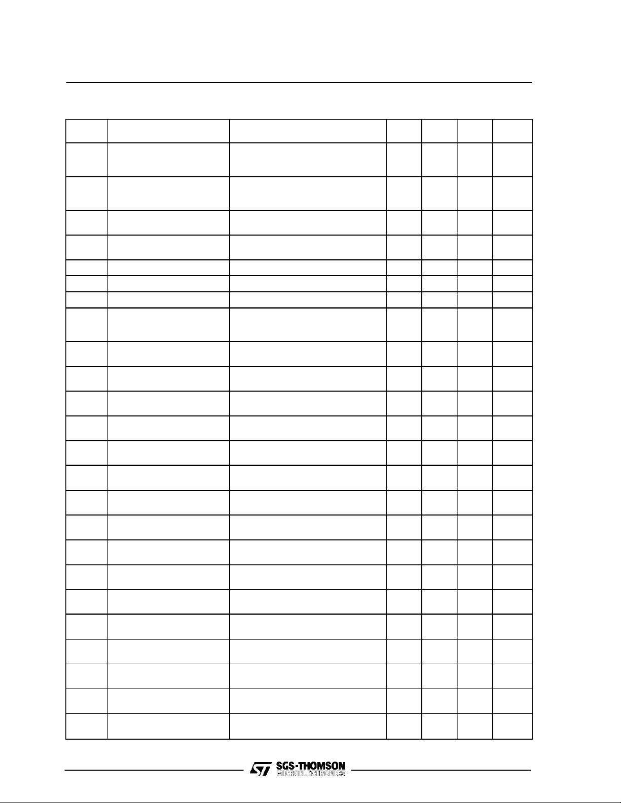
ABSOLUTE MAXIMUM RATINGS
Symbol Parameter Value Unit
V
i
I
rs
June 1994 1/8
DC Input Voltage 44 V
Reset Output Sink Current 20 mA
GS-R51212S/GS-R51515S
ELECTRICALCHARACTERISTICS (T
Symbol
V
Input Voltage
i
GS-R51212S
V
Input Voltage
i
GS-R51515S
l
Input ReflectedCurrent Vi= 24V I
ir
l
Input ReflectedCurrent Vi= 24V I
ir
V
δV
δV
δV
δV
V
l
V
V
V
V
V
V
V
or2,3
OL2,3
OO2,3
I
I
I
I
Enable Input Voltage Vi= 15 to 40V 0 0.8 V
ien
Enable Input Current Vi= 15 to 40V – 1 mA
ien
Inhibit Input Voltage Vi= 15 to 40V 1.2 +Vi V
iinh
Output Voltage 1 Vi= 15 to 40V Io1= 0 to 4.5A
o1
Output Voltage 2
o2
GS-R51212S
Output Voltage 2
o2
GS-R51515S
Output Voltage 3
o3
GS-R51212S
Output Voltage 3
o3
GS-R51515S
Output Ripple
or1
Voltage1
Output Ripple
Voltage2,3
Line Regulation 1 Vi= 15 to 40V Io1= 2.5A
OL1
Line Regulation 2,3 Vi= 15 to 40V
Load Regulation 1 Vi= 24V Io1= 0.5 to 4.5A
OO1
Load Regulation 2,3 Vi= 24V Io1= 2.5A
Output Current 1 Vi= 15 to 40V Vo1= 5.1V
o1
Output Current 2*
o2
GS-R51212S
Output Current 2*
o2
GS-R51515S
Output Current 2*
o2
GS-R51212S
Io2 Output Current 2*
GS-R51515S
Io3 Output Current 3*
GS-R51212S
Parameter Test Conditions Min Typ Max Unit
=25°C unless otherwise specified)
amb
Vo1= +5.1V Io1= 4.5A
15 40 V
Vo2= +12V Io2= 0.35A
Vo3= – 12V Io3= – 0.35A
Vo1= +5.1V
Vo2= +15V Io2= 0.3A
Io1
= 4.5A
15 40 V
Vo3= – 15V Io3= – 0.3A
= Full Load
No external input capacitor
Ci (external) = 100µF/50V
o1,2,3
o1,2,3
= Full Load
0.5 App
0.15 App
+5 +5.1 +5.2 V
Io2= 0 to 0.35/0.3A
Io3= 0 to – 0.35/– 0.3A
Vi= 15 to 40V Io1= 0 to 4.5A
+11.5 +12 +12.5 V
Io2= 0 to 0.35A Io3= 0 to – 0.35A
Vi= 15 to 40V Io1= 0 to 4.5A
+14.5 +15 +15.5 V
Io2= 0 to 0.3A Io3= 0 to – 0.3A
Vi= 15 to 40V Io1= 0 to 4.5A
– 11.5 – 12 – 12.5 V
Io2= 0 to 0.35A Io3= 0 to – 0.35A
Vi= 15 to 40V Io1= 0 to 4.5A
Io2= 0 to 0.3A
= 0 to – 0.3A
Io3
– 14.5 – 15 – 15.5 V
Vi= 24V Io1= 4.5A 30 50 mVpp
Vi= 24V I
= 0.35/0.3A 50 100 mVpp
o2,3
0.5 mV/V
I
= 0.35/0.3A
o2,3
I
o2,3
= 0.35/0.3A
Io1
= 2.5A
1 mV/V
2 mV/A
I
= 0.35/0.3A
o2,3
500 mV/A
I
= 0.05 to 0.35/0.3A
o2,Io3
0 4.5 A
I
= 0 to 0.35/0.3A
o2,3
Vi= 15 to 40V Io1= 0 to 4.5A
0 0.35 A
Vo2= +12V Io3= 0 to – 0.35A
Vi= 15 to 40V Io1= 0 to 4.5A
0 0.3 A
Vo2= +15V Io3= 0 to – 0.3A
Vi= 15 to 40V
Vo2= +12V Io3=0A
Vi= 15 to 40V Io1= 0 to 4.5A
= 0 to 4.5A
Io1
0 0.7 A
0 0.6 A
Vo2= +15V Io3=0A
Vi= 15 to 40V Io1= 0 to 4.5A
0 – 0.35 A
Vo3= – 12V Io2= 0 to 0.35A
2/8
GS-R51212S/GS-R51515S
ELECTRICALCHARACTERISTICS (T
Symbol
I
I
I
I
osck1
I
osc1
I
osc2,3
t
t
R
T
T
* Note: whenoutput current is less than 50mA, outputripple voltage increases due todiscontinuous operation.
Output Current 3*
o3
GS-R51515S
Output Current 3*
o3
GS-R51212S
Output Current 3*
o3
GS-R51515S
Output Current
Limit 1
Output Short-circuit
Current 1
Output Short-circuit
Current 2,3
Soft-start time 10 ms
ss
Reset Time Delay 100 ms
dr
f
Switching Frequency Vi= 15 to 40V Vo1= 5.1V
s
η Efficiency Vi= 24V I
Thermal Resistance 7.5 °C/W
th
Operating Case
cop
TemperatureRange
Storage
stg
TemperatureRange
Parameter Test Conditions Min Typ Max Unit
=25°C unless otherwise specified) (cont’d)
amb
Vi= 15 to 40V Io1= 0 to 4.5A
Vo3= – 15V Io2= 0 to 0.3A
Vi= 15 to 40V Io1= 0 to 4.5A
Vo3= – 12V Io2=0A
Vi= 15 to 40V Io1= 0 to 4.5A
Vo3= – 15V Io2=0A
Vi= 15 to 40V Overload 5.5 A
Vi= 15 to 40V 3 A
Vi= 15 to 40V 0.8 A
Io1= 0.5 to 4.5A
Vo2= +12/+15V Vo3= – 12/– 15V
Io2,Io3= – 0.05 to – 0.35/– 0.3A
= Full Load 78 81 %
o1,2,3
0 – 0.3 A
0 – 0.7 A
0 – 0.6 A
0 +85 °C
– 40 +105 °C
100 kHz
3/8
 Loading...