

Datasheet GS-R415-2, GS-R412-2, GS-R405-2, GS-R424-2, GS-R400V-2 Datasheet (SGS Thomson Microelectronics)
SWITCHING REGULATOR FAMILY
FEATURES
MTBF in excess of 500,000 hours
4A max output current
40V max input voltage
4V max dro p-o ut vo ltage
Soft start
Non-latching short circuit protection
Crow-bar outpu t over volta ge prote ct ion
DESCRIPTION
The GS-R400/2 series is a family of small sized
high current, high voltage step-down switching
regulators.
The integral heatsink allows a large power handling
capability and it provides also an effective shielding
to minimize EMI.
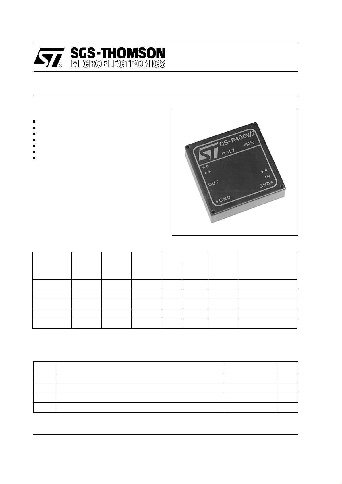
GS-R400/2 Family
SMALL SIZE STEP-DOWN
SELECTION CHART
Type
Ordering
Number
GS-R405/2
GS-R412/2
GS-R415/2
GS-R424/2
GS-R400V/2
Note : Line regulation is measured at I
Load regulation is measured at Vin=Vo+8V and I
Case temperature must be kept below 85° C
Output
Voltage
(V)
5.1 ± 2%
12.0 ± 4%
15.0 ± 4%
24.0 ± 4%
5.1 to 24
9 to 40
16 to 40
19 to 40
28 to 40
V o+4 to 40
Input
Voltage
(V)
=1A.
out
Output
Ripple
(mVpp)
25 2 20 80
50 5 40 85 "
65 6 60 87 "
100 6 80 90 "
25 to 100 2 to 6 20 to 80 80 to 90
=0.5 to 1.5A.
out
Regulation
Line
(mV/V)
Load
(mV/A)
Efficiency
Notes
(%)
Fixed output voltage
Progr. output voltage
ABSOLUTE MAXIMUM RATINGS
Symbol Parameter Value Unit
DC Input Voltage
V
i
Output Current
I
o
T
T
cop
Storage Temperature Range
stg
Operating Case Temperature Range
42 V
4A
– 40 to +105 °C
– 20 to +85 °C
June 1994 1/3

GS- R4 0 0/2 F A M I LY
CONNECTION DIAGRAM AND MECHANICAL DATA
Dimensions in mm Bottom view
Pin 5 GS-R400V/2 only
PIN DESCRIPTION
Pin Function Description
+ Input DC input voltage. Recommended maximum voltage is 40V.
1
Input GND Return for input voltage source.
2
Output GND Return for output c urrent path. Internally connected to pin 2.
3
+ Output Regulated DC output voltage.
4
Program A resistor (<10kΩ) connected between this pin and pin 4 sets the + output voltage of the
5
GS-R400V/2.
ELECTRICAL CHARACTERISTICS (TA = 25°C unless otherwise specified)
Symbol Parameter Test Conditions Min Typ Max Unit
∆Vo/∆T
I
I
S
t
t
V
R
Temperature Stability Vi = Vo+8V Io = 1A
Output Current Vi = Vo+8V
I
o
Current Limit Vi = Vo+8V
oL
Average Input Current Vi = 40V Output Shorted
isc
Switching Frequency Io = 1A
f
s
Supply Voltage Rejection fo = 100Hz Io = 1A
VR
Ripple Voltage Io = 1A
V
r
Soft Start Time
ss
Crowbar Delay Time
cb
Crowbar Intervention Threshold
cth
Thermal Resistance Case to ambient
th
0.2/0.6 mV/°C
0.1 4 A
58A
0.1 0.2 A
100 kHz
4/12 mV/V
25/100 mVpp
10/35 ms
5 µs
Vo•1.25 V
8 °C/W
2/3

GS- R4 0 0/2 F A M I LY
USER NOTES
Input Voltage
The recommended operating maximum DC input
voltage is 40V inclusive of the ripp le voltage.
Case Grounding
The m odule ca se is intern ally con nected t o pin 2
and pin 3.
The PCB area below the module can be used as an
effective sixth side shield against EMI.
Thermal Characteristics
The case -to-ambient thermal resistance of all the
GS-R400/2 modules is about 8°C/W. This produces
a 32°C temperature increase of the module surface
for 4W of internal po wer di ssipat ion .
Dependin g on the am bient tempera ture a nd/or o n
the power dissipation, an additional heatsink or
forced ventilation may be required.
Input Impedance
The modu le has an interna l capacitor connected
between the input pins in order to assure PWM
stability. This capacitor cannot hand le large value s
of high fre quen cy ripple curren t and it can be permanently damaged if the primary energy source
impedance is not adequate.
The use of an external low ESR, high ripple current
capa citor lo cated as cl ose the m odule as possib le
is recommende d.
Suitable capacitors should have a RMS current
capability of 2.5 A
and an ESR of 0,1Ω at 100kHz. When space
V
DC
with a working voltage of 50
RMS
is a limitation a 22µF ce rami c mult ila yer ca pa citor
must be connected to the module input pins.
and the PCB layou t must minimize in jected noise.
The value of th e re sistor is calcula te d by using the
following formula:
= 2.67
R
v
V
5.1
o
− 1
kΩ
Vo can be adjusted betwee n 5.1 and 24V.
Module Protection
The modules are protected against occasional and
permanent short circuits of the output pins to
ground. Du ring short ci rcuit (when th e output current exceeds the maximum value) the output is
automatically disabled. After a fixed time the module
starts again in a soft mode. The cycle is repeated
until the shor t circuit condition is removed.
The module can be permanently damaged if the
case temperature exceeds 85° C
Power Derating Curve
Output Voltage Programming
The GS-R400V/2 output voltage is programmed by
using a resistor.
The resistor must be located very close the module
Information furnished is believed to be accurate and reliable. However, SGS-THOMSON Microelectroni cs assumes no respons ibility for the
consequences of use of such information nor for any infringement of patents or other rights of third parties which may result from its use. No
license is granted by implication or otherwise under any patent or patent rights of SGS-THOMSON Microelectronics. Specification mentioned
in this publication are subject to change without notice. This publication supersedes and replaces all information previously supplied.
SGS-THOMSON Microelect ronics produ cts a re no t a utho rized f or u se as critical c ompo nents in l ife s uppo rt de vices o r sy st ems wi thout expres s
written approval of SGS-THOMSON Microelectronics.
© 1994 SGS-THOMSON Microelectronics – All Rights Reserved
Australia - Brazil - China - France - Germany - Hong Kong - Italy - Japan - Korea - Malaysia - Malta - Morocco - The Netherlands -
Singapore - Spain - Sweden - Switzerland - Taiwan - Thailand - United Kingdom - U.S.A.
SGS-THOMSON Microelectronics GROUP OF COMPANIES
3/3
 Loading...